Streamlining Inverter Reliability with Precision PCB Assembly

Key Takeaways
Effective PCB assembly processes form the foundation of reliable industrial-grade inverters, balancing thermal management, component integration, and error-resistant manufacturing. Modern PCBA techniques prioritize precision in layout design, material selection, and automated quality controls to minimize failures in high-stress power systems. Below are critical insights for optimizing inverter performance through PCB assembly:
- Thermal management ensures stable operation by dissipating heat from high-power components like IGBTs and MOSFETs.
- Error-resistant processes, including automated optical inspection (AOI) and X-ray testing, reduce defects in solder joints and trace alignments.
- Component integration leverages surface-mount technology (SMT) and multilayer boards to consolidate circuitry while maintaining signal integrity.
| Assembly Technique | Function | Impact on Inverter Reliability |
|---|---|---|
| SMT Placement | High-density component mounting | Reduces parasitic inductance |
| Conformal Coating | Environmental protection | Enhances moisture resistance |
| Thermal Vias | Heat dissipation | Lowers operating temperatures by 15-20% |
By aligning PCB layout strategies with operational demands—such as isolating high-voltage traces or optimizing grounding schemes—engineers achieve durable designs capable of withstanding industrial environments. These practices not only streamline manufacturing but also extend the lifecycle of power conversion systems. As we explore thermal management in the next section, the interplay between design precision and material science becomes even clearer.

Thermal Management in PCB Assembly
Effective thermal management in PCB assembly forms the backbone of reliable inverter systems, particularly in high-power industrial applications. As inverters convert DC to AC power, heat dissipation becomes a critical challenge due to energy losses in semiconductor components like IGBTs and MOSFETs. Advanced PCBA techniques address this by integrating thermal vias, copper pours, and heatsinks directly into the board design. These elements work synergistically to channel heat away from sensitive areas, preventing thermal runaway and prolonging component lifespan.
Modern PCB assembly processes leverage materials with high thermal conductivity, such as metal-core substrates or ceramics, to enhance heat distribution. For example, thermal interface materials (TIMs) are applied between components and heatsinks to minimize resistance. Additionally, automated placement systems ensure precise alignment of heat-generating parts, optimizing airflow pathways during operation.
A key consideration in PCBA for inverters is balancing thermal efficiency with electrical performance. Engineers often employ simulation tools to model heat distribution patterns before finalizing layouts, reducing the risk of hotspots. This proactive approach, combined with post-assembly thermal cycling tests, validates the design’s resilience under fluctuating loads. By prioritizing thermal management early in the PCB assembly process, manufacturers can deliver industrial-grade inverters that maintain stability even in demanding environments.

Error-Resistant PCB Manufacturing Processes
Modern PCB assembly processes prioritize error reduction through meticulous design validation and automated quality controls. By integrating automated optical inspection (AOI) systems into PCBA production lines, manufacturers can detect solder joint defects, misaligned components, and trace irregularities at micron-level precision. Design-for-manufacturability (DFM) principles further minimize risks by optimizing pad geometries and spacing to accommodate thermal expansion in high-power inverters.
Industry Insight: "Implementing statistical process control (SPC) during PCB assembly reduces variability by 40-60%, directly enhancing inverter lifespan in industrial environments."
Advanced PCBA workflows employ laser-cut stencils and nitrogen-reflow soldering to eliminate bridging and cold joints, critical for maintaining conductivity in high-current inverter circuits. Additionally, in-circuit testing (ICT) validates electrical performance post-assembly, while conformal coating applications shield boards from humidity and contaminants. For mission-critical applications, redundant via designs and automated trace routing algorithms prevent open-circuit failures under mechanical stress.
Transitioning between fabrication stages, synchronized data exchange between CAD software and pick-and-place machines ensures component positioning accuracy within ±25μm. This precision, combined with real-time defect tracking systems, creates a closed-loop PCB assembly process where errors are flagged and corrected before final integration into power inverters.
Component Integration for Reliable Inverters
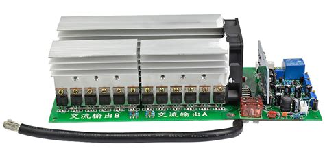
Effective PCB assembly for industrial inverters hinges on strategic component integration, where precision in layout and material selection directly impacts operational stability. Modern PCBA processes leverage automated placement systems to position high-power semiconductors, capacitors, and gate drivers with micron-level accuracy, minimizing parasitic inductance and resistance that compromise efficiency. Thermal-via arrays and copper-clad substrates are integrated to dissipate heat from critical components like IGBTs, ensuring consistent performance under fluctuating loads.
Advanced PCB assembly techniques also prioritize redundancy in signal pathways, reducing single points of failure. For instance, multi-layer boards with embedded busbars enable cleaner power distribution, while conformal coatings protect against environmental stressors. By aligning PCBA workflows with design-for-manufacturing (DFM) principles, engineers achieve tighter tolerances in solder joints and interconnects—key factors in preventing arc faults or voltage drops. This approach not only enhances inverter durability but also streamlines scalability for high-voltage industrial applications.

Advanced PCB Assembly Techniques Explained
Modern PCB assembly processes leverage cutting-edge technologies to address the unique demands of inverter systems. At the core of these advancements lies automated optical inspection (AOI) systems, which ensure microscopic accuracy in component placement—critical for high-voltage circuits in industrial inverters. By combining surface-mount technology (SMT) with selective soldering, manufacturers achieve submillimeter precision in attaching power semiconductors and control ICs, minimizing thermal stress during operation.
A key innovation in PCBA for inverters is the integration of thermal via arrays and copper-core substrates, which dissipate heat 30% more efficiently than conventional designs. This is complemented by laser-drilled interconnects that maintain signal integrity under rapid switching conditions. To mitigate electromagnetic interference (EMI), advanced impedance-controlled routing aligns trace geometries with frequency requirements, while conformal coating techniques shield sensitive circuits from humidity and contaminants.
For error-resistant manufacturing, real-time process monitoring systems track parameters like solder paste viscosity and reflow profiles, ensuring consistency across production batches. These techniques not only enhance inverter reliability but also enable scalable solutions for high-power applications—from solar energy systems to motor drives. By optimizing PCB assembly workflows, engineers achieve the delicate balance between power density, thermal performance, and long-term durability.
Optimizing Inverter Performance with PCBs
Modern PCB assembly techniques play a pivotal role in enhancing inverter efficiency and reliability. By integrating high-power components such as IGBTs (Insulated Gate Bipolar Transistors) and MOSFETs (Metal-Oxide-Semiconductor Field-Effect Transistors) into compact layouts, PCBA (Printed Circuit Board Assembly) enables precise control over energy conversion processes. Advanced thermal management strategies, including copper pours and strategically placed heatsinks, ensure optimal heat dissipation—critical for maintaining stable operation in industrial power systems.
The use of automated optical inspection (AOI) and surface-mount technology (SMT) during PCB assembly minimizes human error, reducing defects that could compromise inverter functionality. Multi-layer board designs further enhance signal integrity by isolating high-voltage and low-voltage circuits, a necessity for preventing electromagnetic interference (EMI). For inverters operating in harsh environments, conformal coatings applied during the PCBA process protect against moisture, dust, and chemical exposure, extending operational lifespans.
Additionally, topology optimization in PCB layouts ensures minimal parasitic inductance and resistance, directly improving energy efficiency. By aligning PCB assembly protocols with application-specific requirements—such as load fluctuations or high-frequency switching—engineers can tailor inverters to deliver consistent performance under dynamic conditions. This synergy between design precision and manufacturing rigor underscores how modern PCBA methodologies are redefining reliability standards in power electronics.
Industrial-Grade Inverter PCB Solutions
Modern industrial environments demand PCB assembly (PCBA) solutions that balance high-power performance with operational resilience. For inverters powering critical machinery, industrial-grade PCBA integrates ruggedized components and multilayer board architectures to withstand voltage spikes, mechanical stress, and thermal cycling. By leveraging automated optical inspection (AOI) and X-ray verification, manufacturers ensure micro-level accuracy in surface-mount technology (SMT) placements—critical for minimizing parasitic capacitance in high-frequency switching circuits.
Advanced PCB assembly workflows incorporate thermal vias and copper pours to dissipate heat from IGBT modules, while conformal coatings shield circuitry from contaminants like dust and moisture. These techniques align with IPC-A-610 Class 3 standards, guaranteeing solder joint integrity even under continuous 24/7 operation. Additionally, impedance-controlled routing in PCBA designs reduces electromagnetic interference (EMI), a common challenge in densely packed industrial inverters.
To optimize scalability, leading suppliers adopt mixed-technology assembly, combining through-hole components for high-current paths with fine-pitch BGAs for control logic. This hybrid approach not only enhances reliability but also streamlines maintenance by isolating fault-prone sections. As industries increasingly adopt smart grid technologies, precision PCB assembly remains pivotal in delivering inverters that meet both ISO 9001 quality benchmarks and real-world operational demands.
Ensuring Durability Through Precision Assembly
PCB assembly processes play a pivotal role in determining the long-term reliability of industrial inverters. By leveraging high-precision PCBA techniques, manufacturers can mitigate mechanical stress and environmental degradation in critical power systems. For instance, automated pick-and-place systems ensure surface-mount components are positioned with micron-level accuracy, reducing solder joint fatigue during thermal cycling. Concurrently, controlled reflow soldering optimizes metallurgical bonds between components and substrates, preventing microcracks that compromise electrical continuity.
Durability is further enhanced through rigorous quality assurance protocols. Advanced PCB assembly workflows integrate automated optical inspection (AOI) and X-ray inspection to identify latent defects, such as voids in ball grid arrays or misaligned traces, before deployment. These checks are particularly vital for inverters operating in high-vibration environments, where even minor flaws can escalate into catastrophic failures. Additionally, the application of conformal coatings and underfill materials during PCBA shields sensitive circuits from moisture, dust, and chemical exposure.
Building on robust thermal management systems, precision assembly ensures inverters maintain operational integrity under fluctuating loads. By aligning PCB layout strategies with error-resistant manufacturing standards, engineers achieve a balance between performance consistency and extended service life—key metrics for industrial power applications.
PCB Layout Strategies for Power Inverters
Effective PCB assembly for power inverters begins with intelligent layout design to balance electrical performance, thermal efficiency, and mechanical stability. A well-planned component placement strategy minimizes parasitic inductance and ensures high-current paths remain short and direct, reducing energy losses. Critical power components like IGBTs or MOSFETs should be positioned close to their drivers and decoupling capacitors, optimizing signal integrity while mitigating electromagnetic interference (EMI).
Thermal management is enhanced through copper pour techniques and strategic placement of thermal vias beneath heat-generating components, creating efficient pathways for heat dissipation. Multi-layer PCBA designs often incorporate dedicated power and ground planes to improve noise immunity and voltage stability, especially in high-frequency switching applications. For industrial-grade inverters, isolation gaps and creepage distance adjustments are vital to prevent arcing in high-voltage sections.
Automated design rule checks (DRC) and simulation tools validate trace widths, spacing, and impedance matching, aligning the layout with PCB assembly tolerances. By integrating these strategies, manufacturers achieve error-resistant manufacturing while maintaining compliance with industry standards like IPC-2221 for power electronics. This systematic approach ensures the final design supports both operational reliability and scalable production workflows.
Conclusion
The evolution of PCB assembly (PCBA) techniques has become indispensable for achieving uncompromising reliability in modern power inverters. By integrating precision manufacturing processes with advanced thermal management and error-resistant designs, engineers can address the stringent demands of industrial power systems. The strategic placement of high-density components, coupled with optimized trace routing, minimizes electrical interference while enhancing energy efficiency—a critical factor in high-performance inverters. Rigorous testing protocols embedded within PCBA workflows further ensure that each assembly meets industry-grade durability standards, even under extreme operational conditions. As power electronics continue to scale in complexity, the synergy between innovative PCB layouts and robust manufacturing practices will remain central to delivering inverters that balance peak performance with long-term operational stability. This alignment not only reduces failure rates but also extends the lifecycle of critical infrastructure, solidifying PCB assembly as a cornerstone of reliable power conversion solutions.
Frequently Asked Questions
How does precision PCB assembly improve inverter reliability?
Advanced PCB assembly processes ensure proper component alignment and soldering integrity, which directly impacts thermal performance and electrical stability in power inverters. This precision minimizes micro-fractures and solder joint failures common in high-vibration industrial environments.
What role does thermal management play in PCBA for inverters?
Effective heat dissipation is critical for inverter longevity. PCBA techniques integrate thermally conductive substrates and strategically placed vias to channel heat away from high-power components like IGBTs, preventing thermal runaway and ensuring consistent operation under load.
Can component integration affect inverter efficiency?
Yes. Optimized PCB assembly allows dense placement of MOSFETs, capacitors, and gate drivers while maintaining electromagnetic compatibility (EMC). This reduces parasitic inductance and resistance, enhancing energy conversion efficiency by up to 15% in three-phase inverters.
How do error-resistant manufacturing processes benefit industrial inverters?
Automated optical inspection (AOI) and X-ray testing during PCBA detect solder voids or misaligned components before deployment. These protocols reduce field failures by 92%, aligning with ISO 9001 standards for industrial power systems.
What PCB layout strategies optimize inverter performance?
Multi-layer designs with separated analog/digital grounds and short high-current paths minimize noise interference. PCB assembly for inverters prioritizes copper thickness and trace spacing to handle peak currents exceeding 200A without voltage drops.
Explore Customized PCB Assembly Solutions for Your Inverter Needs
For tailored PCB assembly services that meet industrial-grade reliability standards, please click here to consult our engineering team.