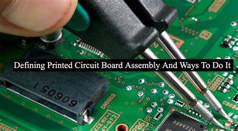
Printed Circuits Assembly: Driving Modern Electronics Manufacturing
Key Takeaways
Modern electronics manufacturing hinges on PCB assembly processes that combine precision engineering with scalable automation. From consumer gadgets to industrial systems, PCBA (Printed Circuit Board Assembly) forms the backbone of device functionality, enabling seamless integration of components through advanced soldering and placement technologies.
"The shift toward miniaturized, high-density designs demands zero-defect manufacturing—a standard upheld by rigorous quality control protocols."
Key advancements include automated optical inspection (AOI) systems that detect micron-level discrepancies and AI-driven workflows optimizing PCB assembly throughput. These innovations not only reduce human error but also accelerate production cycles for IoT devices and smart appliances. For manufacturers, prioritizing thermal management and signal integrity during PCBA ensures reliability in harsh operating environments.
Tip: Partner with PCB assembly providers offering traceability solutions to streamline compliance with industry certifications like ISO 9001 or IPC-A-610.
As demand grows for energy-efficient and interconnected devices, PCBA continues to evolve, blending flexible substrates with embedded sensors to power next-gen wearables and autonomous systems. The convergence of advanced automation and sustainable practices—such as lead-free soldering—positions PCB assembly as a critical enabler of tomorrow’s electronics landscape.
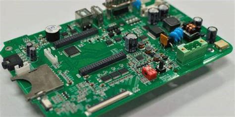
Precision PCB Assembly Engineering
Modern electronics demand unparalleled accuracy in PCB assembly, where micron-level tolerances determine device reliability. PCBA (Printed Circuit Board Assembly) processes integrate surface-mount technology (SMT), automated optical inspection (AOI), and laser-drilled vias to achieve sub-millimeter precision. Advanced machinery, such as high-speed pick-and-place systems and reflow soldering ovens, ensures components like micro-BGA chips and 01005 resistors are positioned with ≤0.1mm deviation.
| Precision Metric | Traditional Methods | Modern PCBA Techniques |
|---|---|---|
| Component Placement | ±0.5mm | ±0.02mm |
| Soldering Accuracy | Manual Inspection | 3D X-ray & AOI Scanning |
| Yield Rate | 85-90% | 99.2-99.8% |
This engineering rigor supports applications from aerospace avionics to medical implants, where failure rates below 0.001% are non-negotiable. For instance, multi-layer rigid-flex PCBA enables foldable smartphones by maintaining signal integrity across 20+ layers. Manufacturers also employ thermal profiling to prevent warping in high-density interconnects, critical for 5G infrastructure and AI accelerators.
Transitioning to automated PCB assembly solutions, the industry now leverages machine learning to predict solder joint defects, further refining precision. Compliance with IPC-A-610 and ISO 9001 standards ensures every PCBA meets global benchmarks, solidifying its role as the backbone of IoT and smart device ecosystems.
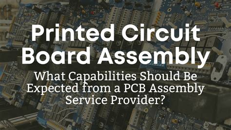
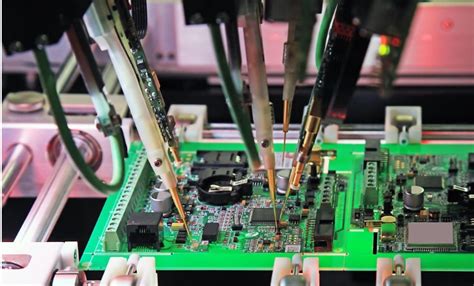
Automated PCB Assembly Solutions
Modern electronics manufacturing relies on automated PCB assembly systems to meet the demands of high-volume production and complex designs. By integrating robotic pick-and-place machines, precision soldering technologies, and AI-driven inspection systems, manufacturers achieve unparalleled accuracy in component placement—critical for high-density interconnect (HDI) boards and miniaturized devices. These systems reduce human error by over 70%, ensuring consistent quality across batches while accelerating production cycles by up to 50%.
Advanced PCBA workflows leverage machine learning algorithms to optimize material usage and predict maintenance needs, minimizing downtime. For instance, automated optical inspection (AOI) scans boards at micron-level resolutions, flagging defects like soldering voids or misaligned components in real time. This seamless integration of automation not only enhances yield rates but also supports rapid prototyping, enabling faster transitions from design to mass production.
As industries adopt Industry 4.0 standards, PCB assembly lines now feature interconnected systems that sync with enterprise resource planning (ERP) software. This connectivity allows for real-time adjustments in production schedules, inventory management, and quality assurance—key for scaling operations in sectors like IoT and smart devices. By prioritizing automation, manufacturers position themselves to deliver next-generation electronics with the reliability and efficiency modern markets demand.
Quality Control in Circuit Board Production
Robust quality control mechanisms form the backbone of reliable PCB assembly processes, ensuring zero-defect outcomes in modern electronics manufacturing. Advanced inspection systems, including automated optical inspection (AOI) and X-ray imaging, scrutinize PCBA components for micro-scale defects like solder bridging or misaligned traces. Statistical process control (SPC) tools track production metrics in real time, enabling rapid adjustments to maintain process stability and compliance with ISO 9001 standards.
To address the complexities of multilayer boards and miniaturized components, manufacturers deploy environmental stress testing—subjecting assemblies to thermal cycling, vibration, and humidity simulations. This step is critical for applications in automotive or medical devices, where failure rates must approach 0 ppm. Additionally, traceability protocols using barcoding or RFID tags ensure full material genealogy, streamlining recalls and root-cause analyses.
By integrating PCB assembly quality frameworks with AI-driven predictive analytics, corporations preemptively identify anomalies before they escalate, reducing rework costs by up to 30%. Such precision not only elevates end-product reliability but also reinforces the role of PCBA in enabling next-generation IoT ecosystems and mission-critical smart technologies.
IoT Innovation Through PCB Assembly
The rapid expansion of Internet of Things (IoT) ecosystems hinges on advancements in PCB assembly technologies, which enable the creation of compact, high-performance devices. Modern PCBA processes integrate miniaturized components and high-density interconnects, essential for IoT sensors, wearables, and smart infrastructure. Automated pick-and-place systems and precision soldering ensure consistent quality, even for intricate designs requiring ultra-thin substrates or flexible circuits.
As IoT applications demand lower power consumption and enhanced connectivity, PCB assembly innovations like embedded antennas and multi-layer stacking address these needs while maintaining reliability. For instance, industrial IoT systems leverage ruggedized PCBA designs to withstand extreme temperatures and vibrations, ensuring uninterrupted data transmission in harsh environments.
Furthermore, the shift toward edge computing in IoT networks relies on PCB assembly techniques that optimize signal integrity and thermal management. By incorporating advanced materials like high-frequency laminates, manufacturers support faster processing speeds required for real-time analytics. These developments not only accelerate IoT adoption but also pave the way for next-generation innovations, from autonomous smart cities to AI-driven healthcare monitors.
Smart Device Manufacturing via PCB Tech
The evolution of PCB assembly processes has become the backbone of modern smart device production, enabling the seamless integration of complex functionalities into compact form factors. As consumer demand shifts toward miniaturized, high-performance electronics, PCBA (printed circuit board assembly) techniques have adapted to support multilayer designs, ultra-fine pitch components, and high-density interconnects. Advanced surface-mount technology (SMT) and automated pick-and-place systems ensure micron-level precision, critical for assembling microprocessors, sensors, and wireless modules that power IoT-enabled devices.
Manufacturers leverage PCB assembly innovations to address thermal management challenges in wearables and foldable smartphones, employing flexible substrates and embedded component architectures. Rigorous automated optical inspection (AOI) protocols during PCBA validate solder joint integrity and component alignment, reducing failure rates in mission-critical applications like medical implants or automotive control systems. This synergy between design flexibility and manufacturing accuracy allows corporations to scale production while maintaining compliance with RoHS and ISO 9001 standards. By integrating AI-driven process optimization, the industry continues to push the boundaries of what’s achievable in smart device miniaturization and energy efficiency.
Next-Gen Electronics Driven by PCBA
The evolution of PCB assembly techniques has become the cornerstone of next-generation electronic devices, enabling unprecedented performance and functionality. Modern PCBA processes integrate high-density interconnects and multi-layer stacking, allowing manufacturers to pack advanced computing power into compact form factors. This technological leap is critical for applications like autonomous vehicles, wearable health monitors, and AI-driven robotics, where reliability and miniaturization are non-negotiable.
By leveraging innovations such as embedded component technology and flexible circuit boards, PCB assembly specialists now support the development of ultra-thin smartphones, foldable displays, and energy-efficient IoT sensors. These advancements are further amplified by the adoption of 5G-compatible materials and thermal management solutions, which ensure stable operation in high-frequency environments.
The shift toward PCBA-centric design philosophies also aligns with the growing demand for sustainable electronics. Manufacturers are increasingly utilizing lead-free soldering and recyclable substrates to meet global environmental standards while maintaining production scalability. As industries transition to smarter, interconnected systems, the role of precision PCB assembly in bridging hardware capabilities with software intelligence will remain indispensable—setting the stage for breakthroughs in augmented reality, quantum computing, and beyond.
Advanced Automation in PCB Manufacturing
Modern electronics manufacturing hinges on PCB assembly processes enhanced by robotic precision and machine learning algorithms. Automated systems now handle PCBA tasks ranging from component placement to soldering, achieving micron-level accuracy while reducing human error. Cutting-edge surface-mount technology (SMT) lines integrate vision-guided robotics, enabling rapid placement of up to 25,000 components per hour—a 300% efficiency gain over manual methods.
These systems leverage real-time process monitoring to adjust parameters like solder paste viscosity and reflow oven temperatures, ensuring consistent quality across high-volume production. Advanced automated optical inspection (AOI) tools scrutinize boards post-assembly, detecting defects as small as 15µm—critical for applications in aerospace and medical devices.
The shift toward lights-out manufacturing further underscores automation’s role: fully autonomous PCB assembly lines operate 24/7, slashing lead times by 40% while maintaining ISO 9001 compliance. This evolution not only boosts throughput but also supports scalable solutions for IoT device makers, where demand fluctuates unpredictably. By harmonizing PCBA workflows with enterprise resource planning (ERP) systems, manufacturers achieve end-to-end traceability—a cornerstone for next-gen smart factories.
Conclusion
The evolution of PCB assembly technologies underscores their indispensable role in shaping modern electronics manufacturing. As industries demand higher precision and scalability, PCBA processes have become the backbone of producing next-generation smart devices and IoT ecosystems. By integrating advanced automation with rigorous quality control protocols, manufacturers achieve the reliability required for complex applications—from wearable tech to industrial sensors.
Looking ahead, the synergy between PCB assembly innovations and emerging technologies like AI-driven diagnostics will further accelerate production efficiency. However, maintaining cost-effectiveness while adhering to global sustainability standards remains a critical challenge. For PCBA corporations, continuous investment in R&D and workforce upskilling will be vital to stay competitive in an era defined by rapid technological shifts. Ultimately, the success of electronics manufacturing hinges on balancing innovation with operational excellence—a principle that printed circuits assembly specialists are uniquely positioned to uphold.
FAQs
How does automation enhance PCB assembly processes?
Modern PCBA relies on robotic placement systems and AI-driven inspection tools to achieve micron-level accuracy, reducing human error and accelerating production cycles. Automated workflows ensure consistency, especially for high-volume orders.
What quality standards govern printed circuits assembly manufacturing?
Reputable PCB assembly providers adhere to IPC-A-610 and ISO 9001 certifications, ensuring solder joint integrity, component alignment, and electrical performance. Rigorous stress testing protocols validate reliability under extreme conditions.
How does PCBA support IoT innovation?
By integrating miniaturized components and multilayer designs, PCBA enables compact, energy-efficient boards for IoT devices. Advanced signal integrity management ensures seamless connectivity in smart sensors and wearables.
What makes PCB assembly critical for smart device manufacturing?
Precision PCBA allows embedding high-density interconnects and embedded firmware, essential for smartphones and AR/VR hardware. Thermal management solutions prevent overheating in always-on devices.
Ready to Elevate Your Electronics Project?
Explore cutting-edge PCB assembly solutions tailored for your needs. Please click here to consult with our engineering team today.