Power PCB Design: Principles, Challenges, and Best Practices
Introduction
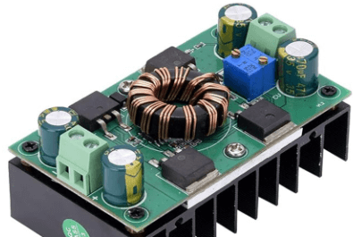
Printed Circuit Boards (PCBs) are the backbone of modern electronics, providing mechanical support and electrical connections between components. When it comes to high-power applications, Power PCBs play a critical role in ensuring efficient energy transfer, thermal management, and reliability. Unlike standard PCBs, power PCBs must handle high currents, voltages, and temperatures while minimizing losses and ensuring safety.
This article explores the fundamentals of Power PCB design, including material selection, layout considerations, thermal management, and common challenges. By understanding these principles, engineers can design robust power electronics for applications such as motor drives, power supplies, electric vehicles, and renewable energy systems.
1. Key Characteristics of Power PCBs
Power PCBs differ from conventional PCBs in several ways:
1.1 High Current Carrying Capacity
Power circuits often carry currents ranging from several amps to hundreds of amps. To prevent excessive resistive losses and overheating, power PCBs require:
- Wider traces to reduce current density.
- Thicker copper layers (e.g., 2 oz/ft² to 6 oz/ft² or more).
- Proper via design to distribute current efficiently.
1.2 High Voltage Isolation
High-voltage applications (e.g., inverters, industrial power supplies) demand:
- Increased creepage and clearance distances to prevent arcing.
- Use of high-dielectric-strength materials (e.g., FR4, polyimide, or ceramic-filled substrates).
1.3 Thermal Management
Power components (e.g., MOSFETs, IGBTs, diodes) generate significant heat. Effective thermal management techniques include:
- Thermal vias to conduct heat away from components.
- Copper pours and heat sinks for better heat dissipation.
- Thermally conductive substrates (e.g., metal-core PCBs or insulated metal substrates (IMS)).
1.4 Low Parasitic Inductance and Resistance
Parasitic elements can cause voltage drops, ringing, and EMI issues. Mitigation strategies include:
- Minimizing loop areas in high-frequency switching circuits.
- Using ground planes to reduce inductance.
- Optimizing component placement to shorten high-current paths.
2. Material Selection for Power PCBs
The choice of PCB material significantly impacts performance, especially in high-power applications.
2.1 Substrate Materials
- FR4: Standard material for low-to-medium power applications. Limited thermal performance.
- High-Tg FR4: Better thermal stability for moderately high-power circuits.
- Metal-Core PCBs (MCPCBs): Aluminum or copper cores for superior heat dissipation (used in LED drivers, power converters).
- Ceramic Substrates (Al₂O₃, AlN): Excellent thermal conductivity for high-power RF and automotive applications.
- Polyimide: High-temperature resistance for aerospace and military applications.
2.2 Copper Thickness
- Standard PCBs use 1 oz/ft² (35 µm) copper.
- Power PCBs often require 2 oz/ft² to 6 oz/ft² (70 µm – 210 µm) or more for high-current traces.
2.3 Dielectric Materials
- High-voltage PCBs need materials with high dielectric strength (e.g., Rogers, Isola).
- Thermal interface materials (e.g., thermally conductive adhesives) improve heat transfer.
3. Power PCB Layout Guidelines
A well-optimized layout is crucial for performance and reliability.
3.1 Trace Width and Current Capacity
The IPC-2152 standard provides guidelines for trace width vs. current. Wider traces reduce resistance and heat generation.
Example:
- A 10 A current may require a 10 mm trace width for 1 oz copper at 20°C temperature rise.
3.2 Component Placement
- Place high-power components (MOSFETs, inductors) near heat sinks.
- Minimize high-current loop areas to reduce parasitic inductance.
- Separate analog and power sections to avoid noise coupling.
3.3 Thermal Design Considerations
- Use thermal vias under power components to transfer heat to inner layers or a heatsink.
- Large copper pours act as heat spreaders.
- Thermal relief pads prevent solder joint cracking during reflow.
3.4 High-Frequency Considerations
- Minimize parasitic inductance in switching circuits (e.g., buck converters).
- Use ground planes to reduce EMI.
- Avoid sharp trace angles (use 45° or curved traces) to prevent impedance discontinuities.
4. Challenges in Power PCB Design
4.1 Thermal Stress and Warping
High temperatures can cause delamination or warping. Solutions:
- Use high-Tg materials.
- Implement symmetrical layer stacking.
4.2 Electromagnetic Interference (EMI)
Switching power circuits generate EMI. Mitigation techniques:
- Proper grounding strategies (star grounding, split planes).
- Shielding (ferrite beads, grounded metal enclosures).
- Filtering (LC filters, snubber circuits).
4.3 Manufacturing Tolerances
Thick copper PCBs require specialized etching and plating processes.
- Ensure proper solder mask application to avoid bridging.
- Controlled impedance routing for high-frequency signals.
5. Applications of Power PCBs
Power PCBs are used in various industries:
- Electric Vehicles (EVs): Battery management systems (BMS), motor controllers.
- Renewable Energy: Solar inverters, wind turbine converters.
- Industrial Power Supplies: High-current DC-DC converters.
- Aerospace & Defense: High-reliability power distribution systems.
6. Future Trends in Power PCB Technology
- Wide-Bandgap Semiconductors (SiC, GaN): Enabling higher efficiency and power density.
- Embedded Power Components: Integrating passive components within the PCB.
- Advanced Thermal Materials: Graphene-enhanced substrates for better heat dissipation.
Conclusion
Designing Power PCBs requires careful consideration of current handling, thermal management, material selection, and EMI control. By following best practices in layout and material choice, engineers can develop reliable, high-performance power electronics for demanding applications.
As technology evolves, innovations in wide-bandgap semiconductors, embedded components, and advanced thermal solutions will further enhance the capabilities of power PCBs, enabling more efficient and compact power systems.