Lead-Free PCBs: The Future of Electronics Manufacturing
Introduction
The electronics industry has undergone significant changes in recent decades, particularly in the materials used for printed circuit board (PCB) manufacturing. One of the most notable shifts has been the transition from lead-based soldering to lead-free (Pb-free) alternatives. This change was driven by environmental concerns, regulatory requirements, and the growing demand for safer and more sustainable electronics.
Lead-free PCBs comply with the Restriction of Hazardous Substances (RoHS) directive, which restricts the use of certain hazardous materials in electrical and electronic equipment. This article explores the development, benefits, challenges, and future trends of lead-free PCB technology.
The Need for Lead-Free PCBs
1. Environmental and Health Concerns
Lead (Pb) has long been used in electronics due to its excellent solderability, low melting point, and reliability. However, lead is a toxic heavy metal that poses severe health risks, including neurological damage, especially in children. When electronic waste (e-waste) is improperly disposed of, lead can leach into soil and water, contaminating ecosystems.
The European Union’s RoHS directive (2002/95/EC), implemented in 2006, was a major regulatory push to eliminate lead and other hazardous substances from electronics. Similar regulations followed in other regions, including China, Japan, and certain U.S. states.
2. Regulatory Compliance
Manufacturers exporting electronics to RoHS-compliant regions must ensure their products meet lead-free standards. Non-compliance can result in legal penalties, market restrictions, and reputational damage. As a result, the industry has shifted toward lead-free soldering and PCB manufacturing.
Lead-Free Solder Alloys
The most common lead-free solder alloys replace traditional tin-lead (Sn-Pb) solder with alternative materials. The key requirements for lead-free solders include:
- Adequate melting temperature (close to Sn-Pb’s 183°C but often higher)
- Good wettability (ability to flow and adhere to surfaces)
- Mechanical strength and reliability
Common Lead-Free Solder Compositions
- Tin-Silver-Copper (SAC Alloys)
- SAC305 (96.5% Sn, 3% Ag, 0.5% Cu): The most widely used lead-free solder, offering a good balance of performance and cost.
- SAC387 (95.5% Sn, 3.8% Ag, 0.7% Cu): Slightly higher silver content improves mechanical strength.
- Tin-Copper (Sn-Cu)
- Sn-0.7Cu: A lower-cost alternative to SAC alloys, commonly used in wave soldering.
- Tin-Silver (Sn-Ag)
- Sn-3.5Ag: Offers good thermal fatigue resistance but is more expensive due to higher silver content.
- Other Alloys (Bi, Zn, In Additives)
- Some alloys incorporate bismuth (Bi) or indium (In) to lower melting points, but these can be more brittle or costly.
Advantages of Lead-Free PCBs
1. Environmental Sustainability
Lead-free PCBs reduce toxic waste and align with global sustainability initiatives such as the Circular Economy and Green Electronics movements.
2. Compliance with Global Regulations
Manufacturers using lead-free processes can access international markets without legal barriers.
3. Improved Thermal Performance (in Some Cases)
Some lead-free solders, like SAC alloys, have higher melting points (217–227°C) compared to Sn-Pb (183°C), which can enhance thermal stability in high-temperature applications.
4. Better Long-Term Reliability (Under Certain Conditions)
Lead-free solder joints can exhibit better resistance to thermal cycling and mechanical stress in some environments.
Challenges of Lead-Free PCBs
Despite their advantages, lead-free PCBs present several technical and economic challenges:
1. Higher Melting Temperatures
Lead-free solders typically require higher reflow temperatures (up to 250°C), which can:
- Increase energy consumption
- Risk thermal damage to sensitive components
- Require more robust PCB substrates
2. Solder Joint Reliability Concerns
- Tin Whiskers: Pure tin coatings can grow conductive whiskers, causing short circuits.
- Brittleness: Some lead-free alloys are more prone to cracking under mechanical stress.
3. Cost Considerations
- Silver-containing alloys (e.g., SAC305) are more expensive than Sn-Pb.
- Higher process temperatures increase manufacturing costs.
4. Process Adjustments
- Manufacturers must optimize reflow profiles to prevent defects like voids or poor wetting.
- Compatibility with existing components and finishes must be verified.
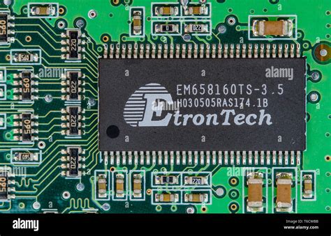
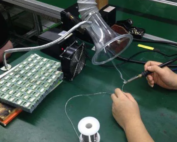
Lead-Free PCB Manufacturing Processes
1. Surface Finishes
The PCB surface finish must be compatible with lead-free soldering. Common options include:
- HASL (Hot Air Solder Leveling) – Lead-Free: Uses tin-copper or tin-nickel alloys.
- ENIG (Electroless Nickel Immersion Gold): Provides excellent oxidation resistance.
- OSP (Organic Solderability Preservative): A cost-effective but less durable option.
- Immersion Silver/Tin: Good for high-frequency applications but can tarnish over time.
2. Reflow Soldering Adjustments
- Higher peak temperatures (240–250°C) are needed for SAC alloys.
- Preheating stages must be carefully controlled to avoid thermal shock.
3. Inspection and Testing
- X-ray inspection helps detect voids in lead-free solder joints.
- Automated Optical Inspection (AOI) ensures proper wetting and alignment.
Future Trends in Lead-Free PCB Technology
1. Advanced Solder Alloys
Research continues into new alloys with:
- Lower melting points (e.g., Sn-Bi-based solders)
- Improved mechanical properties (e.g., nanoparticle-reinforced solders)
2. Sustainable PCB Materials
- Bio-based substrates and recyclable laminates are being explored.
- Halogen-free PCBs reduce additional environmental hazards.
3. Industry 4.0 and Smart Manufacturing
- AI-driven process optimization improves lead-free soldering yields.
- IoT-enabled monitoring ensures consistent quality in PCB production.
4. New Applications (High-Temp, Automotive, Aerospace)
Lead-free PCBs are increasingly used in:
- Electric vehicles (EVs)
- 5G infrastructure
- High-reliability medical devices
Conclusion
The shift to lead-free PCBs represents a critical step toward sustainable and safer electronics manufacturing. While challenges such as higher processing temperatures and reliability concerns remain, ongoing advancements in solder alloys, surface finishes, and manufacturing techniques continue to improve lead-free PCB performance.
As global regulations tighten and consumer demand for eco-friendly products grows, lead-free technology will remain a cornerstone of the electronics industry. Manufacturers must stay ahead by adopting best practices, investing in research, and collaborating with suppliers to ensure compliance and competitiveness in a rapidly evolving market.
By embracing lead-free solutions, the electronics industry can reduce its environmental footprint while delivering high-performance, reliable products for the future.