Advanced PCB Manufacturing Techniques Elevating Electronics Innovation
Key Takeaways
Modern PCB electronics companies leverage pcb assembly advancements to drive innovation across industries. Precision engineering enables micron-level accuracy in pcba processes, ensuring reliable performance for high-frequency and miniaturized devices.
| Technique | Key Benefit | Application Example |
|---|---|---|
| HDI Technology | 20% higher component density | 5G communication modules |
| Flexible Circuits | 40% weight reduction | Wearable medical devices |
| Sustainable Materials | 30% lower carbon footprint | IoT sensor networks |
Tip: When selecting pcb assembly partners, prioritize manufacturers with ISO 13485 certification for mission-critical applications like aerospace or healthcare.
The integration of high-density interconnect (HDI) techniques reduces signal loss while supporting pcba designs with 8+ layers. Advanced laser drilling and automated optical inspection (AOI) systems now achieve defect rates below 0.01%, significantly accelerating prototyping cycles. Sustainable practices, including halogen-free substrates and lead-free finishes, align with global RoHS directives without compromising thermal stability.
For next-gen electronics, pcb electronics companies combine embedded components and 3D-printed circuits to optimize space utilization, enabling 15% smaller form factors in smart devices. These innovations underscore the strategic role of pcba expertise in balancing performance, scalability, and environmental compliance.
Precision Engineering in Modern PCB Manufacturing
Modern PCB assembly processes rely on precision engineering to meet the escalating demands of miniaturized, high-performance electronics. By leveraging nanometer-scale drilling and automated optical inspection (AOI), manufacturers achieve tolerances as tight as ±0.025mm, ensuring flawless alignment for PCBA stages. Advanced laser direct imaging (LDI) systems further enhance trace accuracy, enabling complex multilayer designs with signal integrity critical for 5G and IoT applications.
These techniques minimize electromagnetic interference (EMI) while maximizing component density—a necessity for wearables and medical devices. Real-time data analytics integrated into PCB assembly lines allow iterative refinements, reducing defects by over 30% compared to traditional methods. For PCBA workflows, precision-engineered solder paste application and reflow profiling ensure reliable interconnects even with ultra-fine-pitch components.
The shift toward adaptive manufacturing platforms supports rapid design iterations, bridging the gap between prototyping and mass production. This technical evolution not only accelerates time-to-market but also establishes a foundation for subsequent innovations in HDI and flexible circuitry—key themes explored later in this article.
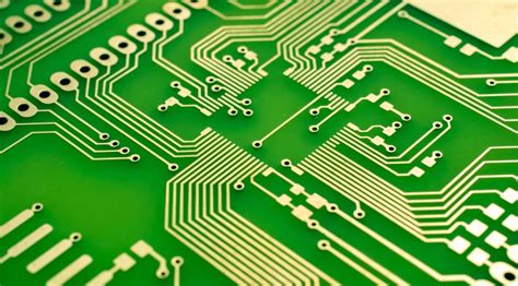
HDI Technology Breakthroughs for Electronics Innovation
The evolution of High-Density Interconnect (HDI) technology has become a cornerstone for advancing modern electronics, enabling unprecedented miniaturization and performance gains. By integrating laser-drilled microvias and stacked via structures, HDI PCBs achieve higher component density while reducing signal loss—a critical requirement for 5G infrastructure, IoT devices, and advanced wearables. Innovations like any-layer buildup architectures allow designers to place components closer together, optimizing space utilization without compromising reliability.
Central to this progress is the synergy between pcb assembly workflows and HDI advancements. Automated pcba processes now support ultra-fine pitch components, ensuring precise placement on densely packed boards. This precision is further enhanced by advanced materials such as low-loss laminates, which improve thermal stability in high-frequency applications. For instance, the adoption of sequential lamination techniques has slashed prototyping cycles, allowing manufacturers to iterate designs faster while maintaining signal integrity.
Moreover, HDI’s role in sustainability cannot be overlooked. Thinner substrates and reduced layer counts lower material waste, aligning with eco-conscious pcb electronics company goals. As industries push toward smarter, smaller devices, HDI remains pivotal in bridging the gap between cutting-edge innovation and scalable production—proving indispensable for next-gen electronics.
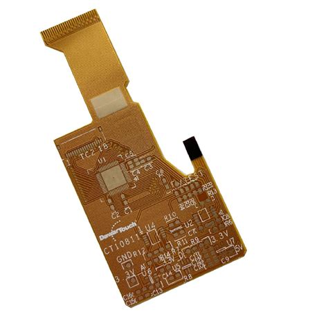
Flexible Circuit Applications in Advanced Devices
As electronics miniaturization accelerates, flexible circuits are revolutionizing device design by enabling three-dimensional integration in space-constrained applications. Unlike traditional rigid boards, these bendable substrates—often paired with HDI technology—allow seamless integration into wearables, medical implants, and aerospace systems. For instance, foldable smartphones leverage ultra-thin polyimide layers to maintain signal integrity across thousands of flex cycles, while implantable medical sensors utilize biocompatible materials for continuous health monitoring.
The shift toward pcb assembly (PCBA) processes optimized for flexible designs has been critical. Advanced pcba workflows now incorporate laser-drilled microvias and anisotropic conductive films to attach components to curved surfaces without compromising reliability. This approach not only reduces weight by up to 70% compared to rigid alternatives but also enhances thermal management in high-density configurations. Automotive innovators, for example, deploy flex circuits in dashboard clusters and LiDAR systems, where vibration resistance and compact layouts are paramount.
Transitioning from prototyping to mass production, manufacturers are adopting hybrid rigid-flex designs that merge high-density PCB solutions with dynamic form factors. Such advancements align with broader industry trends toward sustainable production, as flexible circuits often require fewer materials and generate less waste during pcb assembly. These developments position flexible electronics as a cornerstone for next-generation IoT and AI-driven devices, bridging precision engineering with functional adaptability.
High-Density PCB Solutions for Next-Gen Electronics
The relentless demand for smaller, faster, and more powerful electronic devices has driven the evolution of high-density PCB solutions, which now form the backbone of next-generation electronics. By leveraging HDI (High-Density Interconnect) technology, manufacturers achieve unprecedented component density through microvias, stacked copper layers, and ultra-fine trace widths. These advancements enable miniaturized designs without compromising performance, critical for applications like 5G infrastructure, IoT sensors, and wearable medical devices.
Modern PCB assembly processes integrate automated optical inspection (AOI) and 3D laser drilling to ensure precision in multi-layer stacking, reducing signal loss and crosstalk. For instance, PCBA workflows now incorporate embedded passive components and advanced thermal management materials, addressing heat dissipation challenges in compact layouts. This synergy between design and manufacturing allows engineers to pack more functionality into smaller footprints while maintaining reliability.
Transitioning from traditional methods, high-density PCBs also support heterogeneous integration, combining silicon-based chips with flexible substrates. Such innovations align with the broader industry shift toward system-in-package (SiP) architectures, which demand seamless PCB assembly accuracy. As electronics manufacturers push the boundaries of Moore’s Law, these solutions not only accelerate prototyping cycles but also pave the way for sustainable production by minimizing material waste through optimized layouts.
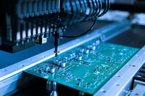
Accelerated Prototyping with Cutting-Edge PCB Methods
Modern electronics development thrives on speed, and advancements in PCB assembly techniques now enable unprecedented prototyping velocities. By integrating automated optical inspection (AOI) systems and AI-driven design validation tools, manufacturers reduce iterative cycles from weeks to days. High-speed PCBA processes, such as laser-direct imaging and automated pick-and-place systems, ensure micron-level accuracy while slashing production lead times.
A critical driver is the adoption of rapid-turn fabrication methods, which combine HDI technology with modular design frameworks. Engineers leverage these innovations to test multiple iterations of complex circuits within a single production batch, minimizing material waste. Additionally, cloud-based collaboration platforms allow real-time adjustments to flexible PCB layouts, synchronizing global teams during prototype refinement.
The shift toward agile prototyping also benefits from hybrid manufacturing approaches. For instance, combining 3D-printed substrates with traditional PCB assembly creates functional prototypes in under 48 hours. This synergy between additive manufacturing and PCBA workflows accelerates validation for IoT sensors, wearable tech, and automotive control modules. By compressing development timelines, businesses gain crucial market advantages—delivering next-gen devices faster without compromising on high-density interconnects or thermal performance.
Sustainable Practices in PCB Electronics Production
The electronics industry is undergoing a critical shift toward environmentally conscious manufacturing, with PCB assembly processes leading the charge. By adopting halogen-free laminates and lead-free soldering techniques, manufacturers minimize toxic waste while maintaining performance standards. Advanced PCBA workflows now integrate energy-efficient machinery, reducing power consumption by up to 30% during high-volume production cycles.
Innovative recycling programs are reclaiming precious metals from discarded boards, with some facilities achieving over 90% material recovery rates. Companies are also leveraging additive manufacturing to reduce raw material waste, particularly in prototyping phases. For instance, laser-direct structuring (LDS) enables precise circuit patterning, eliminating excess copper etching.
Moreover, the adoption of biodegradable substrates in flexible circuits addresses end-of-life disposal challenges. These efforts align with global regulations like RoHS and REACH, ensuring compliance without compromising innovation. As sustainability becomes a strategic priority, PCB electronics companies are proving that eco-friendly practices can coexist with cutting-edge technological advancement, creating a blueprint for greener electronics ecosystems.
Material Science Innovations in Circuit Board Design
Recent breakthroughs in material science are redefining the capabilities of PCB assembly processes, enabling unprecedented performance in modern electronics. Advanced substrates like high-frequency laminates and low-loss dielectrics now support faster signal transmission, critical for 5G infrastructure and high-speed computing. These materials minimize signal degradation while maintaining structural integrity under extreme thermal conditions—a key requirement for PCBA applications in automotive and aerospace systems.
The integration of nanoparticle-enhanced conductive inks has revolutionized circuit patterning, allowing for finer traces and improved conductivity. This innovation directly supports high-density interconnects (HDIs), essential for compact wearable devices and IoT sensors. Additionally, the emergence of flexible hybrid electronics (FHE) combines rigid PCB assembly zones with stretchable polymer substrates, creating bendable circuits for foldable displays and medical wearables.
Sustainability-driven material advancements are equally transformative. Bio-based epoxy resins and halogen-free flame retardants reduce environmental impact without compromising PCBA reliability. These developments align with global RoHS directives while enhancing thermal management in power-intensive applications. By merging novel materials with precision PCB assembly techniques, manufacturers achieve tighter component integration, reduced electromagnetic interference (EMI), and extended product lifespans—paving the way for next-generation electronics.
Optimizing Component Integration Through PCB Tech
Modern electronics demand seamless component integration to balance performance, size, and reliability. Advanced PCB assembly techniques now enable designers to embed high-density interconnects (HDIs) and multi-layer stacking within compact footprints, reducing signal loss while maximizing functionality. Innovations like PCBA (Printed Circuit Board Assembly) automation ensure precise placement of micro-components, such as 01005-sized resistors and ultra-fine-pitch BGAs, which are critical for IoT devices and wearables.
The shift toward 3D packaging and embedded passive components further optimizes space utilization, allowing engineers to integrate power management systems and RF modules into unified layouts. By leveraging PCB assembly workflows with laser-drilled microvias and hybrid materials, manufacturers achieve thermal stability even in high-power applications. These advancements not only enhance electrical performance but also streamline PCBA processes, cutting production cycles by up to 30%.
Transitioning from traditional designs, next-gen PCB tech prioritizes signal integrity through impedance-controlled routing and advanced EMI shielding. This ensures robust integration of mixed-signal components, from analog sensors to high-speed processors, without compromising scalability. As a result, industries ranging from automotive to medical devices gain access to smarter, more interconnected systems built on optimized PCB electronics platforms.
Conclusion
The evolution of PCB assembly processes and material science breakthroughs underscores the transformative trajectory of modern electronics manufacturing. As industries demand higher performance in compact form factors, PCBA (printed circuit board assembly) techniques have become pivotal in balancing miniaturization with functional complexity. Innovations like laser-drilled microvias and sequential lamination enable seamless integration of high-density interconnects, while advancements in flexible PCB substrates support applications ranging from wearable tech to aerospace systems.
Moreover, the shift toward eco-conscious production aligns with global sustainability goals, as manufacturers adopt lead-free soldering and recyclable materials without compromising reliability. By merging HDI technology with intelligent component placement algorithms, pcb electronics company leaders are accelerating prototyping cycles from weeks to days, empowering faster iteration for IoT and AI-driven devices.
Looking ahead, the synergy between advanced simulation tools and multi-layer PCBA workflows will continue to redefine design boundaries, ensuring that next-generation electronics meet both technical and environmental benchmarks. This progression not only elevates product capabilities but solidifies the foundation for scalable, innovation-ready manufacturing ecosystems.
FAQs
How does HDI technology enhance PCB performance in modern electronics?
HDI (High-Density Interconnect) technology enables pcb assembly processes to achieve higher component density by using microvias and finer trace widths. This supports compact designs critical for wearables, IoT devices, and advanced medical equipment.
What advantages do flexible circuits offer in pcba applications?
Flexible circuits, built with polyimide substrates, allow dynamic bending without compromising electrical integrity. They are ideal for aerospace, automotive, and foldable electronics, reducing weight while enhancing durability in pcb assembly workflows.
Are sustainable practices compatible with high-volume PCB production?
Yes. Innovations like halogen-free laminates and lead-free pcba processes align with eco-friendly goals. Advanced recycling systems for copper and substrates further reduce waste, ensuring scalability for industrial applications.
How do material science breakthroughs impact PCB reliability?
New materials, such as low-loss dielectrics and thermally conductive substrates, improve signal integrity and heat dissipation. These advancements enable pcb electronics companies to meet demands for 5G, AI hardware, and high-power devices.
What role does pcb assembly play in accelerating prototyping cycles?
Automated optical inspection (AOI) and 3D printing integration allow rapid design iterations. Combined with simulation-driven pcba workflows, manufacturers can slash prototyping timelines from weeks to days.
Can high-density PCBs support multi-functional IoT devices?
Absolutely. Techniques like embedded component packaging and stacked vias enable pcb electronics companies to integrate sensors, processors, and wireless modules into single boards, optimizing space and power efficiency.
Ready to Transform Your Electronics Project?
For tailored pcb assembly solutions that merge precision engineering with cutting-edge technology, please click here to explore our advanced pcba services.