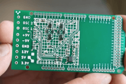
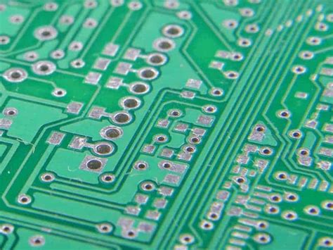
Smart Self-Assembly PCB: The Future of Electronics Manufacturing
Abstract
The electronics industry is undergoing a paradigm shift with the advent of smart self-assembly printed circuit boards (PCBs). These innovative PCBs leverage advanced materials, artificial intelligence (AI), and autonomous robotic systems to assemble themselves with minimal human intervention. This article explores the principles, technologies, benefits, and challenges of smart self-assembly PCBs, highlighting their potential to revolutionize electronics manufacturing.
1. Introduction
Traditional PCB manufacturing involves multiple complex steps, including design, etching, drilling, component placement, and soldering. These processes are labor-intensive, time-consuming, and prone to errors. Smart self-assembly PCBs offer a transformative solution by enabling autonomous assembly through programmable materials, AI-driven robotics, and modular design principles.
Self-assembly is inspired by biological systems, where molecules and cells organize themselves into functional structures. Applying this concept to PCBs could lead to faster production, reduced costs, and enhanced customization. This paper examines the key technologies enabling smart self-assembly PCBs and their implications for the future of electronics.

2. Key Technologies Enabling Smart Self-Assembly PCBs
2.1 Programmable Materials and Nanotechnology
Self-assembly PCBs rely on materials that can autonomously organize into desired structures. Key advancements include:
- Conductive and Self-Aligning Polymers: Materials that can form circuit traces when exposed to specific stimuli (e.g., heat, light, or electric fields).
- Shape-Memory Alloys (SMAs): Components that return to a predefined shape when triggered, enabling self-alignment of connectors.
- Nanoscale Self-Assembly: Using nanoparticles that arrange themselves into conductive pathways, reducing the need for traditional etching.
2.2 AI and Machine Learning for Autonomous Assembly
Artificial intelligence plays a crucial role in optimizing self-assembly processes:
- Computer Vision for Component Alignment: AI-driven cameras and sensors ensure precise placement of components.
- Reinforcement Learning for Error Correction: Machine learning algorithms adapt assembly techniques in real time to minimize defects.
- Generative Design for PCB Layouts: AI generates optimal PCB designs that are easier to self-assemble.
2.3 Modular and Reconfigurable PCB Designs
Self-assembly PCBs often use modular components that can autonomously connect:
- Magnetic and Electrostatic Assembly: Components with embedded magnets or electrostatic properties align themselves without manual intervention.
- Self-Soldering Techniques: Conductive adhesives or thermal-reactive solders activate upon alignment, securing connections automatically.
2.4 Robotics and Micro-Scale Automation
Micro-robots and robotic swarms assist in the self-assembly process:
- Micro-Factories: Small-scale robotic systems that manipulate PCB components at high precision.
- Swarm Robotics: Multiple tiny robots collaborate to assemble complex PCB layouts efficiently.

3. Advantages of Smart Self-Assembly PCBs
3.1 Faster and Scalable Production
- Reduced Assembly Time: Eliminates manual soldering and placement, speeding up manufacturing.
- Mass Customization: Enables on-demand PCB production with minimal reconfiguration.
3.2 Cost Efficiency
- Lower Labor Costs: Reduces dependency on skilled technicians.
- Minimized Material Waste: Precise self-alignment reduces errors and scrap.
3.3 Enhanced Reliability and Precision
- Fewer Human Errors: Automated processes ensure consistent quality.
- Self-Healing Capabilities: Some materials can repair minor circuit breaks autonomously.
3.4 Sustainability
- Reduced Chemical Usage: Eliminates harsh etching chemicals.
- Easier Recycling: Modular designs allow for component reuse.
4. Challenges and Limitations
4.1 Technical Barriers
- Complexity in Large-Scale Assembly: Current self-assembly techniques work best for small PCBs.
- Material Limitations: Not all electronic components are compatible with self-assembly methods.
4.2 High Initial Development Costs
- R&D Investment: Significant funding is required for advanced materials and AI integration.
4.3 Standardization and Compatibility Issues
- Lack of Industry Standards: Uniform protocols for self-assembly PCBs are still evolving.
5. Future Prospects and Applications
5.1 Space and Military Electronics
- Self-Repairing PCBs for Satellites: Autonomous repair in harsh environments.
5.2 Wearable and Flexible Electronics
- Self-Assembling Biomedical Sensors: Custom-fit wearable health monitors.
5.3 Consumer Electronics
- On-Demand Device Manufacturing: Smartphones and IoT devices assembled at home.
6. Conclusion
Smart self-assembly PCBs represent a groundbreaking advancement in electronics manufacturing. By integrating AI, nanotechnology, and robotics, these systems promise faster, cheaper, and more sustainable production. While challenges remain, ongoing research and industry adoption could soon make self-assembling PCBs a mainstream reality, reshaping how we design and manufacture electronic devices.


