The Evolution and Future Trends of Consumer Electronics PCBs
Introduction to Consumer Electronics PCBs
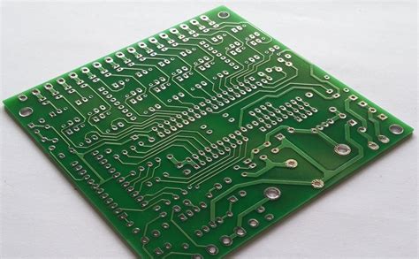
Printed Circuit Boards (PCBs) form the foundational infrastructure of modern consumer electronics, serving as the central nervous system that connects and supports all electronic components. In consumer electronics, PCBs have evolved from simple single-layer boards to highly complex, multi-layered systems that enable the sophisticated functionality we expect from today’s devices.
The consumer electronics PCB market has grown exponentially alongside the rapid expansion of personal technology devices. From smartphones and tablets to smart home devices and wearable technology, PCBs have become smaller, more efficient, and more capable while maintaining reliability and reducing production costs. This evolution has been driven by continuous innovation in materials, manufacturing processes, and design methodologies.
Historical Development of Consumer Electronics PCBs
The journey of PCBs in consumer electronics began in the mid-20th century when they replaced point-to-point wiring in radios and television sets. These early PCBs were simple phenolic boards with copper traces on one side, a far cry from today’s sophisticated designs. The 1970s and 1980s saw the introduction of double-sided boards and through-hole technology, enabling more complex circuits in devices like early home computers and gaming consoles.
A significant leap occurred in the 1990s with the widespread adoption of surface-mount technology (SMT). This allowed components to be mounted directly onto the surface of PCBs rather than requiring leads to pass through holes. SMT enabled smaller components, higher component density, and automated assembly processes—critical developments for the emerging mobile phone and portable electronics markets.
The 21st century has brought about revolutionary changes with high-density interconnect (HDI) technology, flexible PCBs, and rigid-flex designs. These advancements have made possible the ultra-thin smartphones, foldable devices, and compact wearables that dominate today’s consumer electronics landscape.
Current Technologies in Consumer Electronics PCBs
High-Density Interconnect (HDI) PCBs
HDI technology represents the current gold standard for most high-end consumer electronics. Characterized by finer lines and spaces (under 100 microns), smaller vias (under 150 microns), and higher connection pad density, HDI PCBs allow for more components to be packed into smaller areas. This technology enables the slim form factors of modern smartphones while maintaining or increasing functionality.
HDI boards typically feature microvias—laser-drilled holes that can be as small as 15-30 microns in diameter—which allow for complex multilayer interconnections. Stacked and staggered microvia configurations provide three-dimensional routing possibilities that were unimaginable with conventional through-hole vias.
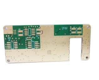
Flexible and Rigid-Flex PCBs
The demand for wearable devices and foldable smartphones has propelled flexible PCB technology to the forefront. Flexible PCBs use substrates made of polyimide or similar materials that can bend, fold, and flex without damaging the conductive traces. These boards enable innovative form factors and can withstand hundreds of thousands of bending cycles in properly designed applications.
Rigid-flex PCBs combine the best of both worlds, incorporating rigid sections for component mounting and flexible sections for three-dimensional packaging. This technology is particularly valuable in space-constrained devices where traditional wiring harnesses would be impractical.
Embedded Component Technology
An emerging trend in consumer electronics PCBs is the embedding of passive components (resistors, capacitors) and even some active components directly within the PCB layers. This approach saves surface space, reduces the overall thickness of the assembly, and can improve electrical performance by minimizing parasitic inductance from component leads.
Advanced Materials
While FR-4 remains the workhorse material for many consumer PCBs, high-frequency applications (such as 5G devices) often require specialized materials with better dielectric properties. Materials like Rogers, Teflon, and ceramic-filled PTFE provide stable dielectric constants and low loss tangents at high frequencies. For thermal management, metal-core PCBs (especially aluminum-based) are finding increasing use in high-power LED lighting and power electronics within consumer products.
Design Considerations for Consumer Electronics PCBs
Miniaturization Challenges
The relentless push for smaller devices presents numerous design challenges. As traces become narrower, issues like signal integrity, crosstalk, and thermal management become more critical. Designers must carefully consider trace width and spacing, impedance control, and power distribution networks to ensure reliable operation.
Signal Integrity in High-Speed Designs
Modern consumer devices operate at increasingly high frequencies, with processor clocks in the GHz range and memory interfaces pushing data rates beyond 10 Gbps. At these speeds, PCB traces behave like transmission lines, requiring careful impedance matching and termination to prevent signal reflections and maintain signal integrity.
Differential pair routing, length matching, and careful via design become essential in high-speed designs. The use of ground planes and proper stack-up configuration helps control electromagnetic interference (EMI) and maintain signal quality.
Power Delivery Networks
As processors become more powerful while operating at lower voltages, power delivery becomes a critical design factor. Modern System-on-Chip (SoC) designs may require multiple voltage rails with strict tolerance requirements. PCB designers must create low-impedance power distribution networks with adequate decoupling to prevent voltage droop during high-current transients.
Thermal Management
Heat dissipation is a growing concern in compact consumer devices. PCB design plays a crucial role in thermal management through:
- Strategic placement of thermal vias to conduct heat to inner layers or opposite sides of the board
- Use of thermal pads and exposed copper areas for better heat transfer
- Careful component placement to avoid hot spots
- In some cases, incorporation of metal cores or heat spreaders within the PCB structure
Design for Manufacturing (DFM) and Design for Test (DFT)
With consumer electronics facing intense cost pressure, DFM considerations are paramount. Design choices that may work electrically but are difficult or expensive to manufacture can significantly impact profitability. Similarly, DFT considerations ensure that boards can be properly tested during production to maintain quality standards.
Manufacturing Processes and Challenges
Precision Fabrication
Modern consumer electronics PCBs require extremely precise fabrication processes. Laser direct imaging (LDI) has largely replaced traditional photolithography for patterning fine features, allowing for higher resolution and better registration accuracy. Laser drilling enables the creation of microvias with diameters as small as 25 microns.
Surface Finishes
The choice of surface finish impacts solderability, durability, and cost. Common finishes for consumer electronics include:
- Electroless Nickel Immersion Gold (ENIG): Provides a flat surface ideal for fine-pitch components
- Immersion Silver: Lower cost than ENIG with good solderability
- Organic Solderability Preservative (OSP): Economical but less durable
- Electroless Nickel Electroless Palladium Immersion Gold (ENEPIG): For demanding applications requiring multiple wire bonding
Assembly Challenges
The miniaturization of components presents significant assembly challenges. 01005 (0.4mm × 0.2mm) and even smaller components require highly accurate pick-and-place machines and precise solder paste application. Bottom-terminated components like QFNs and BGAs demand careful thermal profile management during reflow to prevent tombstoning or voiding.
Quality Control and Testing
Automated optical inspection (AOI), X-ray inspection, and automated test equipment have become essential for maintaining quality in high-volume consumer electronics production. Flying probe testers and boundary scan techniques help verify board functionality without requiring custom test fixtures.
Emerging Trends and Future Directions
Additive Manufacturing of PCBs
While traditional PCB fabrication remains subtractive (removing copper to create traces), additive processes are gaining traction. Inkjet printing of conductive traces and fully additive processes could enable rapid prototyping and customization while reducing material waste.
Integration with Other Technologies
PCBs are increasingly being integrated with other technologies:
- Molded interconnect devices (MIDs) combine injection-molded plastic with conductive traces
- Printed electronics allow for ultra-low-cost, flexible circuits for simple applications
- 3D-printed electronics promise to merge mechanical and electrical design in single processes
Sustainable PCB Manufacturing
Environmental concerns are driving changes in PCB materials and processes:
- Lead-free solders and halogen-free laminates
- Water-based cleaning processes replacing chemical solvents
- Recycling programs for end-of-life electronics
- Development of biodegradable substrate materials
Advanced Packaging Technologies
As traditional PCB scaling faces physical limits, advanced packaging technologies are emerging:
- Fan-out wafer-level packaging (FOWLP) redistributes dies on a carrier for higher I/O density
- 3D IC stacking with through-silicon vias (TSVs) enables vertical integration
- System-in-Package (SiP) solutions combine multiple dies in a single package
AI in PCB Design and Manufacturing
Artificial intelligence is beginning to transform PCB development:
- AI-assisted routing tools can optimize complex designs
- Machine learning algorithms predict and prevent manufacturing defects
- Automated design rule checking and verification
Conclusion
The consumer electronics PCB industry continues to evolve at a rapid pace, driven by demands for smaller, faster, and more feature-rich devices. From the materials used to the manufacturing processes employed, every aspect of PCB technology is undergoing continuous improvement and innovation.
As we look to the future, challenges such as thermal management in increasingly dense designs, signal integrity at higher frequencies, and the need for sustainable manufacturing practices will shape the next generation of PCB technologies. The integration of PCBs with emerging technologies like flexible electronics, advanced packaging, and additive manufacturing promises to unlock new possibilities in consumer product design.
The humble PCB, often overlooked by end users, remains at the heart of the consumer electronics revolution. Its ongoing evolution will continue to enable the innovative devices that shape our digital lives, proving that even in an era of system-on-chips and advanced packaging, the printed circuit board remains an indispensable technology.