The Evolution and Significance of PCB Microvias in Modern Electronics
Introduction
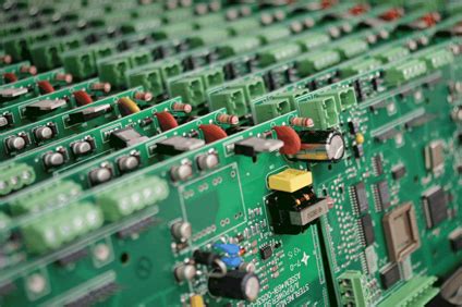
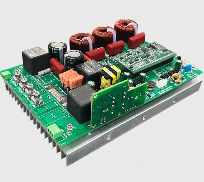
Printed Circuit Boards (PCBs) are the backbone of modern electronics, enabling the interconnection of components in devices ranging from smartphones to aerospace systems. As electronic devices become smaller, faster, and more complex, the demand for high-density interconnect (HDI) PCBs has surged. One of the key innovations facilitating this trend is the microvia—a small, laser-drilled hole used to create connections between different layers of a PCB.
This article explores the evolution, manufacturing processes, advantages, challenges, and future trends of microvias in PCB design.
1. What Are Microvias?
Microvias are tiny holes drilled into PCBs to establish electrical connections between different layers. Unlike traditional through-hole vias, which span the entire board, microvias are typically:
- Blind vias: Connecting an outer layer to one or more inner layers but not passing through the entire board.
- Buried vias: Linking inner layers without reaching the outer surfaces.
Key Characteristics:
- Diameter: Typically less than 150 µm (6 mils).
- Aspect Ratio: Usually 1:1 (depth equals diameter), though advanced processes allow higher ratios.
- Formation: Created using laser drilling (UV, CO₂, or excimer lasers) due to their precision.
2. Evolution of Microvias
The development of microvias has been driven by the need for miniaturization and higher performance in electronics.
Historical Context:
- 1980s-1990s: Through-hole vias dominated PCB manufacturing.
- Late 1990s: The rise of HDI PCBs led to the adoption of microvias.
- 2000s: Laser drilling became standard, enabling smaller and more reliable microvias.
- 2010s-Present: Stacked and staggered microvias allowed for even greater interconnect density.
Industry Standards:
- IPC-6012: Defines acceptability criteria for microvias.
- IPC-2226: Provides design guidelines for HDI/microvia PCBs.
3. Manufacturing Processes for Microvias
Producing microvias involves several critical steps:
A. Laser Drilling
- UV Lasers: Preferred for precision (wavelength ~355 nm).
- CO₂ Lasers: Used for larger holes but less precise for microvias.
- Excimer Lasers: High precision but expensive.
B. Desmearing & Cleaning
After drilling, debris (smear) must be removed via:
- Plasma Etching
- Chemical Desmearing
C. Metallization (Plating)
- Electroless Copper Deposition: Provides initial conductive layer.
- Electroplating: Builds up copper thickness for reliability.
D. Filling & Capping
Microvias can be filled with:
- Conductive Epoxy (for electrical continuity).
- Non-Conductive Fill (for structural support).
- Copper Plating (for high-reliability applications).
4. Advantages of Microvias
Microvias offer several benefits over traditional vias:
A. Space Efficiency
- Enable higher routing density, crucial for compact devices like smartphones and wearables.
B. Improved Signal Integrity
- Shorter interconnects reduce parasitic capacitance and inductance.
- Essential for high-speed digital and RF applications (5G, AI processors).
C. Enhanced Thermal Management
- Better heat dissipation due to optimized via placement.
D. Design Flexibility
- Support complex multilayer designs (e.g., stacked microvias).
5. Challenges & Reliability Concerns
Despite their advantages, microvias present several challenges:
A. Thermal Stress & Cracking
- Repeated thermal cycling (e.g., in automotive or aerospace applications) can cause microvia cracks.
- Solutions: Use of filled vias, improved materials (low-CTE dielectrics).
B. Plating Quality Issues
- Incomplete plating can lead to open circuits.
- Solutions: Advanced electroplating techniques, process control.
C. Cost Considerations
- Laser drilling and precise alignment increase manufacturing costs.
D. Reliability Testing
- IPC standards require extensive testing (thermal cycling, cross-section analysis).
6. Future Trends in Microvia Technology
The evolution of microvias continues as PCB technology advances:
A. Smaller & Higher Aspect Ratio Vias
- Sub-50 µm microvias for next-gen HDI PCBs.
- Aspect ratios > 1:1.5 for deeper interconnects.
B. Advanced Materials
- Low-loss dielectrics for high-frequency applications.
- Flexible PCBs with microvias for foldable electronics.
C. Additive Manufacturing (3D Printing)
- Potential for fully printed microvias, reducing waste and cost.
D. AI & Automation in PCB Design
- AI-driven design optimization for microvia placement.
Conclusion
Microvias have revolutionized PCB design, enabling the miniaturization and performance enhancements required by modern electronics. While challenges such as thermal reliability and manufacturing costs persist, ongoing advancements in laser drilling, materials science, and automation promise to further improve microvia technology.
As the demand for smaller, faster, and more reliable electronics grows, microvias will remain a cornerstone of PCB innovation, shaping the future of consumer electronics, automotive systems, and beyond.