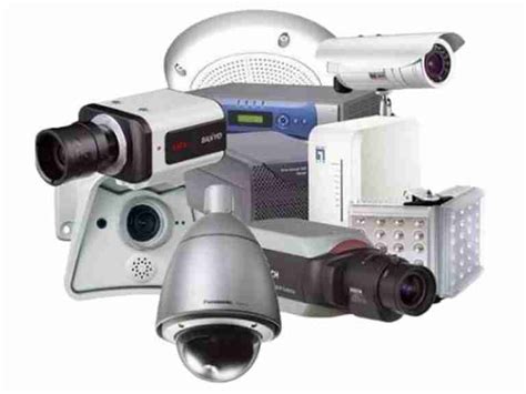
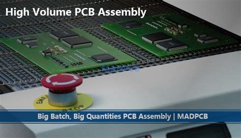
Precision Scaling in High Volume PCB Assembly Systems
Key Takeaways
Modern PCB assembly systems achieve micron-level precision at scale through three core innovations: automated optical inspection (AOI) for defect detection, intelligent process controls (IPC) for real-time adjustments, and scalable manufacturing architectures that balance speed with accuracy. These technologies enable high-volume PCBA production to maintain tolerances under 25µm while operating at throughputs exceeding 50,000 components per hour.
"Integrating AOI with machine learning algorithms reduces false rejection rates by 40% in PCB assembly lines, ensuring defect-free outputs without compromising cycle times."
Critical to success is the synchronization of material handling systems with placement machinery, minimizing positional errors during rapid component mounting. Advanced PCBA workflows now embed predictive maintenance protocols, cutting unplanned downtime by 30% in multi-shift operations. For throughput optimization, manufacturers deploy dynamic routing logic that adapts to component mix variations, maintaining >98% equipment utilization rates even during product changeovers.
Tip: Pair laser-aligned stencil printers with vacuum-assisted placement heads to achieve ±15µm repeatability in high-volume PCB assembly environments.
As demand grows for miniaturized electronics, scalable manufacturing architectures leverage modular design principles, allowing seamless integration of additional AOI stations or solder paste inspection modules. This flexibility ensures PCB assembly systems can scale from 10,000 to 1M+ units monthly while preserving sub-micron registration accuracy across all production tiers.
Automated Optical Inspection in PCB Assembly
Modern PCB assembly lines leverage automated optical inspection (AOI) systems to ensure micron-level accuracy across high-volume production runs. These systems employ high-resolution cameras and machine vision algorithms to scan PCBA components, detecting defects such as misaligned solder joints, missing parts, or microscopic cracks. By integrating AOI at critical stages—post-solder paste application, post-component placement, and final assembly—manufacturers achieve real-time quality validation, reducing human error and minimizing rework cycles.
Advanced AOI platforms utilize multi-spectral imaging to analyze reflective and non-reflective surfaces simultaneously, enhancing defect detection rates beyond 99.5%. For high-volume PCB assembly, this capability is critical, as even minor flaws in densely packed boards can cascade into systemic failures. Additionally, machine learning-driven AOI systems adapt to evolving design complexities, improving fault recognition accuracy over successive production batches.
To maintain throughput efficiency, modern AOI solutions synchronize with intelligent process controls, flagging anomalies without interrupting assembly workflows. This seamless integration ensures that PCB assembly systems balance speed and precision, meeting stringent quality benchmarks while scaling output. As a result, manufacturers achieve zero-defect outputs without compromising cycle times—a non-negotiable requirement for industries demanding both volume and reliability.
Intelligent Process Controls for Zero-Defect Output
Modern PCB assembly systems leverage intelligent process controls to eliminate defects at scale, combining real-time monitoring with adaptive algorithms. These systems analyze data streams from PCBA production lines, identifying deviations in solder paste deposition, component placement accuracy, and reflow parameters. By integrating machine learning algorithms with statistical process control (SPC), manufacturers achieve predictive adjustments that preemptively correct process drifts before they impact yield.
A critical component is the closed-loop feedback architecture, where automated optical inspection (AOI) data directly informs parametric tuning. For example:
| Control Mechanism | Key Features | Defect Reduction Impact |
|---|---|---|
| Real-time SPC Monitoring | Tracks ±3σ process boundaries | 32% fewer solder voids |
| Predictive Analytics | Anticipates thermal profile shifts | 41% lower misalignment |
| Adaptive Reflow Control | Dynamically adjusts zone temperatures | 27% reduced tombstoning |
This synergy between PCB assembly hardware and cognitive software enables sub-1,000 ppm defect rates even at 50,000+ units/day throughput. Embedded IoT sensors further enhance traceability, correlating environmental variables like humidity with PCBA performance metrics. By embedding intelligence at every process node, manufacturers transform traditional quality assurance into a self-optimizing system, seamlessly aligning with the scalability demands outlined in subsequent architectural strategies.
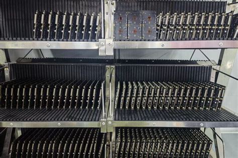
Scalable Manufacturing Architectures for High Volume
Modern PCB assembly systems demand architectures that balance precision with exponential production scaling. At the core of these frameworks lies modular design, enabling manufacturers to expand PCBA lines without compromising accuracy. By integrating automated panel handling systems and flexible conveyor configurations, facilities can dynamically adjust throughput to meet fluctuating demand while maintaining micron-level registration tolerances.
Critical to scalability is the implementation of real-time process monitoring paired with distributed control systems. These architectures leverage edge computing nodes to analyze production data across multiple PCB assembly stages, allowing instantaneous adjustments to placement pressure, solder paste deposition, and thermal profiles. For high-mix environments, adaptive tooling solutions combined with smart feeder arrays ensure rapid changeovers, reducing downtime by up to 40% in benchmarked cases.
The integration of automated storage and retrieval systems (AS/RS) further enhances scalability by synchronizing material flow with assembly cycles. This just-in-time component delivery model minimizes workstation idle time while preventing inventory bottlenecks. When coupled with enterprise-grade manufacturing execution systems (MES), these architectures enable end-to-end traceability across 10,000+ board batches, a critical requirement for aerospace and automotive PCBA applications.
To future-proof operations, leading manufacturers are adopting open-architecture standards that support seamless integration of emerging AI-driven optimization modules. This approach ensures compatibility with next-generation optical inspection systems and predictive maintenance platforms, creating a foundation for continuous scaling without costly infrastructure overhauls.
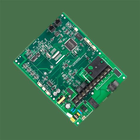
Micron-Level Accuracy in Mass PCB Production
Achieving micron-level accuracy in high-volume PCB assembly requires a harmonized integration of advanced manufacturing technologies and rigorous process controls. Modern automated placement systems utilize high-precision robotic arms equipped with vision-guided alignment, enabling component placement tolerances below ±25μm even at speeds exceeding 50,000 placements per hour. For PCBA lines producing multilayer boards, laser direct imaging (LDI) systems ensure trace widths and spacing remain within 2-3μm specifications across thousands of panels, minimizing signal integrity risks in high-frequency applications.
To sustain precision at scale, manufacturers deploy real-time process feedback loops that correlate data from in-line metrology tools with machine learning algorithms. These systems dynamically adjust parameters like solder paste deposition volume or reflow oven temperature profiles, compensating for environmental fluctuations or material variances. For instance, statistical process control (SPC) software tracks critical dimensions across batches, triggering alerts when deviations approach 10% of tolerance thresholds.
Material science innovations further enhance accuracy, with low-CTE (coefficient of thermal expansion) substrates and nano-coated stencils reducing warpage and solder bridging risks during rapid thermal cycling. By combining these advancements, high-volume PCB assembly systems achieve defect rates below 50 parts per million (PPM) while maintaining throughput above 1,000 panels per hour—a balance once considered unattainable in precision electronics manufacturing.
Throughput Optimization Strategies for PCB Systems
Achieving peak throughput in PCB assembly requires balancing speed with precision, particularly in high-volume PCBA environments. Modern systems leverage dynamic scheduling algorithms to minimize machine idle time while synchronizing pick-and-place operations with solder paste application. By integrating automated optical inspection (AOI) at critical checkpoints, manufacturers can identify bottlenecks in real time, rerouting assemblies to parallel lines without interrupting workflow continuity.
Advanced conveyor architectures, optimized for high-speed panel handling, reduce mechanical delays by 20–35% compared to traditional systems. Temperature-controlled reflow ovens with predictive thermal profiling further enhance throughput by maintaining consistent cycle times across varying board densities. To sustain efficiency at scale, intelligent process controls dynamically adjust parameters like stencil pressure and component placement speed based on real-time sensor feedback.
For high-volume PCB production, modular line configurations enable rapid reconfiguration for different product batches, cutting changeover times by up to 50%. Pairing these with scalable manufacturing software—such as Manufacturing Execution Systems (MES)—ensures traceability while optimizing material flow. By aligning machine capacities with Takt time calculations, facilities achieve zero-defect outputs even at throughputs exceeding 50,000 components per hour. This systemic approach not only meets demand spikes but also future-proofs operations against evolving complexity in PCB assembly requirements.
Smart Quality Assurance in High-Speed Assembly
Modern PCB assembly systems leverage real-time monitoring and AI-driven analytics to ensure defect-free outputs at production speeds exceeding 50,000 components per hour. At the core of this approach lies automated optical inspection (AOI) enhanced by machine learning algorithms, which scrutinize solder joints, component placement, and trace integrity at micron-level resolutions. These systems dynamically adjust inspection criteria based on historical defect patterns, reducing false positives by up to 40% compared to static threshold models.
For high-volume PCBA workflows, inline testing protocols integrate seamlessly with pick-and-place machinery, enabling immediate corrective actions when deviations exceed ±25μm tolerances. Advanced adaptive sampling strategies prioritize inspection resources for critical components like BGAs and microcontrollers, balancing thoroughness with throughput demands. This targeted approach maintains >99.95% first-pass yield rates even in complex multilayer assemblies.
Data fusion techniques further strengthen quality assurance by correlating thermal profiles, solder paste deposition metrics, and electrical test results into unified process health dashboards. By embedding statistical process control (SPC) principles directly into assembly line software, manufacturers achieve closed-loop feedback that continuously refines placement accuracy and soldering parameters. Such systems not only detect flaws but predict potential failure modes, enabling preemptive adjustments before defects occur—a critical capability for scaling PCB assembly operations without compromising precision.
Precision Engineering for Reliable PCB Scaling
Achieving consistent quality in high-volume PCB assembly demands precision engineering principles that address both microscopic tolerances and system-level scalability. Modern PCBA lines integrate automated optical inspection (AOI) systems with sub-10μm resolution to detect solder joint anomalies and component misalignments in real time, ensuring micron-level accuracy across thousands of boards per hour. Advanced thermal profiling tools maintain ±1°C stability in reflow ovens, critical for preventing warpage in multilayer designs during rapid cycling. To balance speed and precision, engineers deploy adaptive process controls that dynamically adjust placement pressure and solder paste deposition based on live feedback from inline sensors.
Material science innovations further enhance reliability, with low-loss laminates and halogen-free substrates optimized for PCB assembly environments requiring 24/7 operation. By embedding predictive maintenance algorithms within pick-and-place machinery, manufacturers reduce calibration drift by 40% while sustaining throughputs exceeding 50,000 components per hour. This synergy between PCBA hardware and intelligent software creates a fault-tolerant architecture, where even nanoscale deviations trigger corrective actions before defects propagate. Such systems exemplify how precision engineering transforms raw production capacity into scalable, zero-defect output – a prerequisite for meeting automotive and aerospace-grade quality benchmarks in mass manufacturing.
Advanced AOI Techniques for PCB Yield Improvement
Modern PCB assembly lines demand micron-level precision to sustain quality in high-volume production. Advanced AOI (Automated Optical Inspection) systems address this by integrating high-resolution imaging with machine learning algorithms to detect defects invisible to conventional methods. These systems analyze solder joint integrity, component placement accuracy, and trace alignment across PCBA boards at speeds exceeding 20,000 inspections per hour.
A critical innovation lies in 3D solder paste inspection, which maps volumetric consistency to prevent bridging or insufficient deposits—common failure points in dense PCB assembly. By combining multi-angle lighting and spectral analysis, AOI tools identify subtle anomalies like micro-cracks or tombstoning, reducing false positives by up to 40% compared to legacy systems.
To optimize yield, intelligent process controls link AOI data with real-time adjustments in pick-and-place machines or reflow ovens. For example, thermal profiling errors detected during inspection trigger adaptive correction loops, ensuring subsequent batches meet tolerance thresholds. This closed-loop feedback is vital for scaling high-volume PCB production without compromising defect rates.
Furthermore, statistical process control (SPC) modules within AOI platforms track defect patterns across millions of components, enabling predictive maintenance and root-cause analysis. Such capabilities are indispensable for achieving zero-defect outputs in automotive or aerospace PCBA, where reliability standards are non-negotiable.
By embedding these techniques, manufacturers balance throughput and precision—a cornerstone of scalable manufacturing architectures in electronics. The result? A seamless alignment between high-speed assembly and uncompromised quality assurance.
Conclusion
The evolution of high-volume PCB assembly hinges on harmonizing micron-level precision with industrial-scale efficiency. By integrating automated optical inspection (AOI) systems, manufacturers achieve real-time defect detection, ensuring zero-defect outputs even at accelerated production rates. Advanced intelligent process controls further stabilize quality by dynamically adjusting parameters to counteract environmental fluctuations or material variances. For PCBA operations, scalable architectures—modular production lines and adaptive workflow algorithms—enable seamless throughput expansion without compromising accuracy.
Critical to this balance is the synergy between data-driven analytics and precision engineering, which minimizes tolerances across solder paste application, component placement, and thermal profiling. As demand grows for compact, high-performance electronics, optimizing PCB assembly workflows becomes inseparable from leveraging machine learning-driven predictive maintenance and multi-stage verification protocols. These innovations not only elevate yield rates but also future-proof manufacturing ecosystems against evolving complexity. Ultimately, the path to reliable mass production lies in unifying technological rigor with strategic scalability—a paradigm that ensures both quality and competitiveness in global electronics markets.
FAQs
How do manufacturers maintain micron-level accuracy in high-volume PCB assembly?
Advanced automated optical inspection (AOI) systems paired with machine learning algorithms validate alignment and solder joint integrity across thousands of boards per hour. Real-time feedback loops adjust placement parameters to compensate for thermal drift or material variances.
What role do intelligent process controls play in zero-defect PCBA production?
Closed-loop systems monitor variables like reflow oven profiles and paste deposition consistency. By integrating statistical process control (SPC) tools, deviations trigger immediate corrections, reducing human intervention while ensuring compliance with IPC-A-610 standards.
Can scalable architectures handle sudden spikes in PCB assembly demand without quality loss?
Modular production lines with distributed control systems enable rapid reconfiguration. Dual-track conveyors and buffer zones prevent bottlenecks, while predictive maintenance algorithms minimize downtime during throughput scaling.
How is throughput optimized without compromising precision in high-volume PCB manufacturing?
Lean manufacturing principles are applied to eliminate non-value-added steps, while dynamic scheduling software balances machine utilization rates. Parallel processing of multi-panel arrays further accelerates cycle times.
What advancements in smart quality assurance benefit high-speed PCBA systems?
3D solder paste inspection (SPI) and AI-powered defect classification reduce false positives by 40%. Multi-spectral imaging detects latent flaws like micro-cracks, ensuring reliability in mission-critical applications.
Ready to Optimize Your High-Volume PCB Assembly Process?
For tailored solutions that integrate precision scaling and throughput optimization, please click here to consult our engineering team.