Printed Circuit Board Assemblies: Design, Manufacturing, and Applications
Introduction
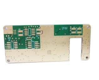
Printed Circuit Board Assemblies (PCBAs) are the backbone of modern electronics, forming the foundation of nearly all electronic devices, from smartphones to industrial machinery. A PCBA consists of a printed circuit board (PCB) populated with electronic components such as resistors, capacitors, integrated circuits (ICs), and connectors. The assembly process involves soldering these components onto the PCB to create a functional electronic circuit.
This article explores the key aspects of PCBAs, including their design considerations, manufacturing processes, testing methods, and applications across various industries.
1. PCBA Design Considerations
Designing a PCBA involves multiple critical steps to ensure functionality, reliability, and manufacturability.
1.1 Schematic Design
The first step is creating a schematic diagram that defines the electrical connections between components. Engineers use Electronic Design Automation (EDA) tools like Altium Designer, KiCad, or Cadence OrCAD to draft schematics.
1.2 PCB Layout
Once the schematic is finalized, the PCB layout is designed. Key considerations include:
- Layer Stackup: Single-layer, double-layer, or multilayer PCBs (4+ layers) depending on complexity.
- Component Placement: Optimizing placement for signal integrity, thermal management, and manufacturability.
- Trace Routing: Ensuring proper trace width, spacing, and impedance control for high-speed signals.
- Power and Ground Planes: Essential for reducing noise and providing stable power distribution.
1.3 Design for Manufacturing (DFM)
DFM guidelines help minimize production defects. These include:
- Adequate solder mask and silkscreen clearances.
- Proper pad sizes for surface-mount components.
- Avoiding tombstoning (uneven solder paste causing component misalignment).
2. PCBA Manufacturing Process
The PCBA manufacturing process involves several stages:
2.1 PCB Fabrication
The bare PCB is manufactured through processes such as:
- Substrate Preparation: Using materials like FR-4, polyimide, or Rogers material for high-frequency applications.
- Copper Etching: Removing unwanted copper to form conductive traces.
- Drilling and Plating: Creating vias and through-holes for electrical connections.
- Solder Mask and Silkscreen Application: Protecting the board and labeling components.
2.2 Component Sourcing
Procuring high-quality components is crucial. Supply chain challenges, such as counterfeit parts, must be managed through trusted suppliers.
2.3 Assembly Techniques
Two primary assembly methods are used:
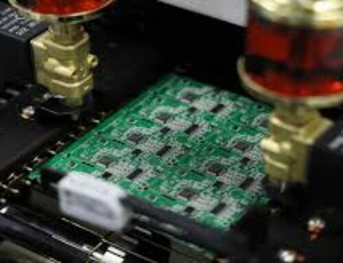
2.3.1 Surface-Mount Technology (SMT)
- Components are placed directly onto the PCB using pick-and-place machines.
- Reflow soldering melts solder paste to form electrical connections.
- Ideal for small, high-density designs (e.g., smartphones).
2.3.2 Through-Hole Technology (THT)
- Components with leads are inserted into drilled holes and soldered manually or via wave soldering.
- Used for high-reliability applications (e.g., military and aerospace).
2.4 Soldering and Reflow
- Reflow Oven: Heats the PCB to melt solder paste, forming permanent connections.
- Wave Soldering: Used for THT components, where the PCB passes over a molten solder wave.
2.5 Conformal Coating
A protective layer (e.g., acrylic, silicone, or urethane) is applied to prevent moisture, dust, and chemical damage.
3. Testing and Quality Control
Ensuring PCBA reliability involves rigorous testing:
3.1 Automated Optical Inspection (AOI)
Cameras inspect solder joints and component placement for defects like bridging or misalignment.
3.2 In-Circuit Testing (ICT)
Electrical probes verify component values and connectivity.
3.3 Functional Testing
The assembled PCB is powered on to validate performance under real-world conditions.
3.4 Environmental Stress Testing
- Thermal Cycling: Checks performance under extreme temperatures.
- Vibration Testing: Ensures durability in mechanical stress environments.
4. Applications of PCBAs
PCBAs are used across multiple industries:
4.1 Consumer Electronics
- Smartphones, laptops, and wearables rely on high-density PCBAs.
4.2 Automotive
- Engine control units (ECUs), infotainment systems, and ADAS (Advanced Driver Assistance Systems) use robust PCBAs.
4.3 Medical Devices
- PCBA reliability is critical in pacemakers, MRI machines, and diagnostic equipment.
4.4 Industrial Automation
- PLCs (Programmable Logic Controllers) and robotics depend on high-performance PCBAs.
4.5 Aerospace and Defense
- Ruggedized PCBAs withstand extreme conditions in satellites and military hardware.
5. Future Trends in PCBA Technology
5.1 Miniaturization
- High-density interconnect (HDI) PCBs enable smaller, more powerful devices.
5.2 Flexible and Rigid-Flex PCBs
- Used in foldable smartphones and wearable technology.
5.3 IoT and Smart Manufacturing
- PCBAs with embedded sensors enable real-time monitoring in Industry 4.0 applications.
5.4 Sustainable Manufacturing
- Lead-free soldering and recyclable materials reduce environmental impact.
Conclusion
Printed Circuit Board Assemblies are fundamental to modern electronics, enabling the functionality of devices across industries. Advances in design, manufacturing, and testing continue to push the boundaries of performance and reliability. As technology evolves, PCBAs will play an even greater role in innovations such as 5G, AI, and the Internet of Things (IoT).
Understanding the complexities of PCBA design and production is essential for engineers, manufacturers, and businesses aiming to develop cutting-edge electronic products. By adhering to best practices in design, assembly, and testing, the industry can ensure the continued growth and reliability of electronic systems worldwide.