Breadboard vs. PCB: Understanding the Differences and Applications in Electronics Prototyping
Introduction to Prototyping Platforms
In the world of electronics design and development, two fundamental platforms dominate the prototyping landscape: breadboards and printed circuit boards (PCBs). These essential tools serve distinct purposes in the electronics workflow, each offering unique advantages that cater to different stages of the development process. Breadboards, with their temporary, solderless connections, provide an ideal environment for initial circuit experimentation and quick modifications. PCBs, on the other hand, represent the professional, permanent implementation of a circuit design ready for production or deployment.
Understanding the characteristics, strengths, and limitations of both breadboards and PCBs is crucial for electronics engineers, hobbyists, and students alike. This comprehensive examination will explore the technical aspects, practical applications, and evolutionary relationship between these two fundamental electronics platforms, providing valuable insights for anyone involved in circuit design and implementation.
Breadboards: The Foundation of Rapid Prototyping
Physical Structure and Design
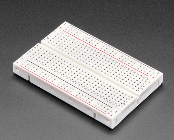
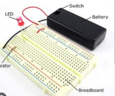
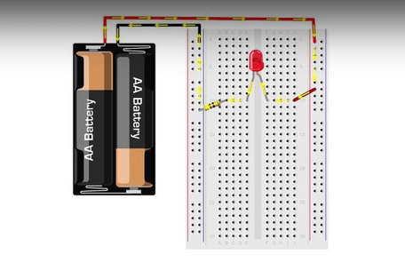
Breadboards, also known as solderless breadboards or prototyping boards, feature a distinctive plastic housing with a grid of holes connected by internal metal clips. The standard breadboard layout consists of two sets of parallel rails running along the sides (typically for power distribution) and multiple rows of interconnected tie points in the center area for component placement. These boards are designed with a 0.1-inch (2.54 mm) spacing between holes to accommodate standard dual in-line package (DIP) integrated circuits and through-hole components.
The internal architecture of a breadboard reveals its functionality: metal spring clips beneath each hole grip component leads when inserted, creating electrical connections without requiring soldering. The central trench separates two sets of five interconnected holes (often called a “node”), allowing ICs to straddle the divider with pins accessible on both sides. Power rails run the length of the board, providing convenient access to voltage and ground connections throughout the circuit.
Advantages of Breadboard Prototyping
Breadboards offer several compelling advantages that make them indispensable for certain stages of electronics development:
- Rapid Iteration: Engineers can quickly assemble, modify, and disassemble circuits without soldering, enabling fast experimentation and debugging.
- Component Reusability: Parts can be easily removed and reused in other projects, reducing material costs during the prototyping phase.
- Visual Circuit Layout: The physical arrangement of components on the breadboard provides an intuitive representation of the circuit schematic.
- Real-time Modification: Design changes can be implemented immediately during testing, allowing for interactive development.
- Beginner-Friendly: The solderless nature makes breadboards ideal for students and electronics newcomers learning circuit fundamentals.
Limitations and Challenges
Despite their utility, breadboards present several limitations that affect their use in more advanced applications:
- Contact Reliability: Over time or with frequent use, the metal clips can loosen, leading to intermittent connections that are difficult to diagnose.
- Frequency Constraints: The inherent capacitance and relatively long connection paths limit breadboards to low-frequency applications (typically below 10-20 MHz).
- Power Handling: Most breadboards are rated for only moderate current levels (usually around 1A per connection point), restricting high-power applications.
- Physical Size: Complex circuits may require multiple breadboards connected together, leading to bulky, disorganized arrangements.
- Noise Sensitivity: The open structure makes breadboard circuits more susceptible to electromagnetic interference compared to PCBs.
Printed Circuit Boards: The Professional Standard
PCB Composition and Manufacturing
Printed Circuit Boards represent the industry-standard platform for electronic circuit implementation. A basic PCB consists of a non-conductive substrate (typically FR-4 fiberglass) with thin layers of copper foil laminated to one or both sides. Through a process of etching, drilling, and plating, these copper layers are transformed into precise conductive pathways that interconnect electronic components according to the designed schematic.
Modern PCBs can range from simple single-layer boards to complex multi-layer designs with dozens of conductive layers separated by insulating material. Advanced manufacturing techniques allow for features like plated through-holes, vias, surface-mount technology (SMT) pads, and even embedded components. The finished board typically receives a solder mask coating (usually green) that insulates the copper traces while leaving component pads exposed, and often includes a silkscreen layer for component labels and identifiers.
Advantages of PCB Implementation
PCBs offer numerous advantages that make them essential for production-quality electronics:
- Reliability: Soldered connections and permanent traces provide stable, long-term performance with minimal contact issues.
- High-Density Layout: Multi-layer designs and surface-mount components allow for compact, space-efficient circuit implementations.
- Signal Integrity: Controlled impedance traces, proper grounding schemes, and shielding options enable high-frequency operation.
- Manufacturability: PCB designs can be mass-produced with consistent quality using automated assembly processes.
- Durability: Properly designed PCBs can withstand mechanical stress, vibration, and harsh environmental conditions better than breadboard implementations.
PCB Design Considerations
Creating effective PCB designs requires attention to several critical factors:
- Schematic Capture: The circuit must be accurately represented in electronic design automation (EDA) software before layout begins.
- Component Placement: Strategic arrangement of parts minimizes trace lengths, reduces noise, and optimizes thermal management.
- Routing: Trace width, spacing, and pathing affect signal quality, power delivery, and electromagnetic compatibility.
- Layer Stackup: Multi-layer boards require careful planning of signal, power, and ground layers for optimal performance.
- Design Rules: Manufacturing constraints (minimum trace width, hole sizes, etc.) must be followed to ensure producibility.
Transitioning from Breadboard to PCB
When to Make the Transition
The decision to move from breadboard prototyping to PCB implementation depends on several factors:
- Design Maturity: When the circuit design has been thoroughly tested and no major changes are anticipated.
- Performance Requirements: When the circuit needs to operate at higher frequencies or with greater reliability than a breadboard can provide.
- Production Needs: When multiple copies of the circuit are required for deployment or testing.
- Form Factor Constraints: When the circuit must fit within specific size or shape requirements.
- Environmental Considerations: When the circuit will be subjected to vibration, moisture, or other challenging conditions.
The Conversion Process
Transitioning a design from breadboard to PCB involves several key steps:
- Schematic Development: Creating a formal schematic diagram based on the breadboard prototype.
- Component Selection: Choosing appropriate packages (through-hole or surface-mount) for PCB implementation.
- Layout Design: Arranging components and routing traces in PCB design software.
- Design Verification: Checking for errors and performing signal integrity analysis if needed.
- Manufacturing Preparation: Generating Gerber files and other documentation required for board fabrication.
Prototyping PCBs
For projects that fall between breadboard prototyping and full custom PCB production, several intermediate options exist:
- Perfboards: Pre-drilled boards with copper pads or strips for point-to-point soldering.
- Stripboards: Similar to perfboards but with continuous copper strips for easier connections.
- Prototype PCB Services: Quick-turn, low-cost PCB fabrication suitable for small quantities.
- Universal PCBs: Boards with standard patterns that can accommodate various circuit designs.
Advanced Topics and Future Directions
Breadboard-Compatible PCBs
The line between breadboards and PCBs has blurred with the development of hybrid solutions:
- Breakout Boards: Small PCBs that adapt modern components (like QFN packages or modules) to breadboard-compatible pinouts.
- Shields: PCB modules designed to plug directly into breadboard power rails or microcontroller boards.
- Interposer Boards: Adapters that allow surface-mount components to be used in breadboard environments.
Educational Implications
The progression from breadboard to PCB mirrors the learning journey in electronics education:
- Conceptual Understanding: Breadboards help students visualize circuit connections and experiment freely.
- Design Discipline: PCB design teaches precision, planning, and attention to manufacturing constraints.
- Professional Preparation: Modern EDA tools give students experience with industry-standard workflows.
Emerging Technologies
Both prototyping platforms continue to evolve with new technologies:
- Breadboard Innovations: Self-contained units with built-in power supplies, signal generators, and measurement tools.
- PCB Advances: Flexible circuits, 3D-printed electronics, and embedded components are expanding PCB capabilities.
- Virtual Prototyping: Simulation tools allow for initial testing before any physical implementation.
Conclusion: Choosing the Right Tool for the Job
Breadboards and PCBs serve complementary roles in electronics development, each excelling in different phases of the design process. Breadboards remain unparalleled for initial concept validation, educational purposes, and quick iterative testing where flexibility is paramount. PCBs, while requiring more upfront design effort, provide the reliability, performance, and professional finish needed for final implementations.
The skilled electronics practitioner understands when to leverage each platform’s strengths, transitioning smoothly from the experimental freedom of breadboarding to the precision engineering of PCB design. As prototyping technologies continue to advance, both breadboards and PCBs will maintain their essential positions in the electronics workflow, adapting to new components, design methodologies, and manufacturing techniques while continuing to serve as the fundamental building blocks of circuit implementation.
Ultimately, mastery of both breadboard prototyping and PCB design represents a critical skillset for anyone serious about electronics development, enabling the transformation of abstract circuit concepts into functional, reliable electronic devices.