Understanding Source PCB: Design, Manufacturing, and Applications
Introduction
Printed Circuit Boards (PCBs) are the backbone of modern electronics, providing mechanical support and electrical connections for electronic components. Among the various types of PCBs, Source PCBs play a crucial role in many applications, particularly in power electronics, embedded systems, and communication devices. This article explores the fundamentals of Source PCBs, their design considerations, manufacturing processes, and key applications.
1. What is a Source PCB?
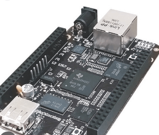
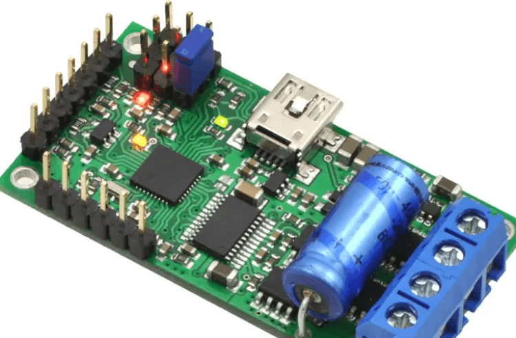
A Source PCB is a specialized type of printed circuit board designed to manage power distribution, signal integrity, and thermal performance in electronic circuits. The term “Source” often refers to its role in power supply circuits, where it acts as the primary board delivering power to other components or subsystems.
Key Characteristics of Source PCBs:
- High Current Handling: Designed to manage significant power loads.
- Thermal Management: Incorporates heat dissipation techniques like copper pours, thermal vias, and heatsinks.
- Signal Integrity: Ensures minimal noise and interference in power delivery.
- Robust Construction: Often uses thicker copper layers and high-quality substrates for durability.
2. Design Considerations for Source PCBs
Designing a Source PCB requires careful attention to electrical, thermal, and mechanical factors. Below are some critical design considerations:
A. Layer Stackup and Material Selection
- Substrate Material: FR-4 is common, but high-power applications may require materials like Rogers, Aluminum-backed PCBs, or Ceramic substrates for better thermal performance.
- Copper Thickness: Thicker copper (2oz to 6oz) is used for high-current traces to reduce resistance and heat buildup.
- Multi-Layer Design: Often employs 4+ layers with dedicated power and ground planes for better EMI shielding.
B. Power Distribution Network (PDN)
- Wide Traces: Power traces must be wide enough to handle current without excessive heating.
- Decoupling Capacitors: Placed near ICs to stabilize voltage and reduce noise.
- Via Placement: Multiple vias help distribute current evenly and reduce inductance.
C. Thermal Management
- Thermal Vias: Help transfer heat from high-power components to other layers or heatsinks.
- Copper Pours: Large copper areas act as heat spreaders.
- Heatsinks & Fans: Used in high-power applications to maintain safe operating temperatures.
D. Signal Integrity & EMI Control
- Ground Planes: Essential for reducing electromagnetic interference (EMI).
- Proper Routing: High-speed signals should be routed away from power lines to avoid crosstalk.
- Shielding: Metal shields or grounded copper layers can block interference.
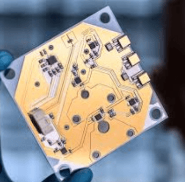
3. Manufacturing Process of Source PCBs
The manufacturing of Source PCBs follows standard PCB fabrication processes but with additional steps for high-power and thermal requirements.
A. PCB Fabrication Steps
- Design & Gerber File Generation
- CAD software (e.g., Altium, KiCad) is used to create the PCB layout.
- Gerber files are generated for manufacturing.
- Material Preparation
- Substrate (e.g., FR-4) is selected based on thermal and electrical needs.
- Copper foil is laminated onto the substrate.
- Drilling & Plating
- Holes for vias and component leads are drilled.
- Plating ensures electrical connectivity between layers.
- Etching & Trace Formation
- Unwanted copper is etched away, leaving conductive traces.
- Thicker copper requires specialized etching techniques.
- Solder Mask & Silkscreen Application
- Solder mask prevents short circuits and protects traces.
- Silkscreen adds component labels.
- Surface Finishing
- ENIG (Electroless Nickel Immersion Gold), HASL (Hot Air Solder Leveling), or OSP (Organic Solderability Preservative) is applied for solderability.
- Testing & Quality Control
- Electrical testing (e.g., flying probe test) checks for shorts or open circuits.
- Thermal testing ensures heat dissipation is adequate.
B. Special Considerations for Source PCBs
- Heavy Copper PCBs: Require modified etching and plating processes.
- Thermal Management Features: Additional steps for heatsink attachment or embedded cooling.
- High-Frequency Materials: Specialized laminates for RF/microwave applications.
4. Applications of Source PCBs
Source PCBs are widely used in industries where power delivery and thermal management are critical. Some key applications include:
A. Power Supplies & Converters
- Switched-Mode Power Supplies (SMPS): Used in AC/DC and DC/DC converters.
- Uninterruptible Power Supplies (UPS): Ensures stable power delivery in critical systems.
B. Automotive Electronics
- Electric Vehicle (EV) Power Systems: Manages battery management systems (BMS) and motor controllers.
- LED Lighting Drivers: Provides efficient power to automotive lighting.
C. Industrial Electronics
- Motor Control Boards: Used in robotics and automation.
- High-Power Inverters: Converts DC to AC in solar power systems.
D. Consumer Electronics
- Gaming Consoles & PCs: High-performance motherboards with robust power delivery.
- Smart Home Devices: Power management in IoT devices.
E. Telecommunications
- Base Stations & RF Amplifiers: Requires stable power and thermal management.
- 5G Infrastructure: High-frequency PCBs with efficient power distribution.
5. Future Trends in Source PCB Technology
As electronics evolve, Source PCBs must adapt to new challenges:
A. Higher Power Densities
- GaN & SiC Devices: Wider adoption of Gallium Nitride (GaN) and Silicon Carbide (SiC) transistors for efficient high-power circuits.
- Embedded Cooling: Liquid cooling or microchannel heatsinks integrated into PCBs.
B. Advanced Materials
- Flex & Rigid-Flex PCBs: For compact and high-reliability designs.
- High-Tg Materials: Better thermal stability for extreme environments.
C. Smart Power Management
- AI-Optimized Power Delivery: Machine learning algorithms for dynamic power distribution.
- Energy Harvesting PCBs: Integrating solar or kinetic energy recovery.
D. Miniaturization & 3D Printing
- HDI (High-Density Interconnect) PCBs: Finer traces and microvias for compact designs.
- 3D-Printed Electronics: Additive manufacturing for custom PCB shapes.
6. Conclusion
Source PCBs are essential for modern electronics, particularly in power-intensive applications. Their design requires careful consideration of electrical, thermal, and mechanical factors to ensure reliability and efficiency. With advancements in materials, manufacturing techniques, and power electronics, Source PCBs will continue to play a pivotal role in emerging technologies like electric vehicles, 5G, and AI-driven systems.
By understanding the principles of Source PCB design and manufacturing, engineers can develop more efficient and robust electronic systems, paving the way for future innovations.