Gerber Fabrication Best Practices for PCB Manufacturing Success

Key Takeaways
When preparing Gerber files for PCB manufacturing, understanding foundational principles ensures your design transitions smoothly from concept to production. Start by confirming your PCB manufacturing companies’ specific requirements—these often include layer stack-up details, solder mask preferences, and drill file specifications. Using modern formats like RS-274X/X2 eliminates ambiguity in aperture definitions, while ODB++ or IPC-2581 provides richer data for complex designs.
Tip: Always request a Design-for-Manufacturing (DFM) checklist from your fabricator to align your files with their capabilities and avoid costly revisions.
Here’s a quick comparison of popular Gerber formats:
| Format | Key Features | Best For |
|---|---|---|
| RS-274X/X2 | Standardized apertures, embedded data | Simple to mid-complexity PCBs |
| ODB++ | Layer stack-up, netlist inclusion | High-density designs |
| IPC-2581 | Intelligent data exchange | Full supply chain integration |
To minimize PCB manufacturing cost, verify drill files include tool sizes and plating requirements. Misaligned drill charts or missing layers can delay production, impacting your PCB manufacturing business timelines. Use automated validation tools to check for overlaps, copper slivers, or unconnected nets before submission.
Collaboration is critical: share prototypes or 3D models early to identify thermal or mechanical conflicts. By prioritizing clear communication and rigorous file checks, you’ll streamline workflows and reduce the risk of respins—safeguarding both quality and budget.

Gerber File Best Practices Guide
When preparing files for PCB manufacturing, precision begins with understanding how Gerber formats serve as the universal language between designers and PCB manufacturing companies. Start by verifying your design software exports RS-274X/X2 files—the industry-standard format that includes embedded apertures and layer polarity data. This eliminates ambiguities and reduces PCB manufacturing cost by minimizing back-and-forth clarifications.
Always double-check layer assignments and ensure copper pours, solder masks, and silkscreen layers are explicitly labeled. Misaligned layers can lead to costly re-spins, directly impacting your PCB manufacturing business timelines. Use a design rule checker (DRC) to flag potential issues like trace spacing violations or missing drill files before submission.
Collaborate early with your fabricator to confirm their specific requirements, such as file naming conventions or stack-up details. Tools like Gerber validation software help automate checks, ensuring your files meet IPC-2581 or ODB++ compatibility if needed. Remember, even minor oversights in annular ring sizes or drill-to-copper clearances can derail production.
Finally, archive all design iterations with clear versioning. This practice not only streamlines future revisions but also builds trust with PCB manufacturing partners by demonstrating systematic professionalism. By mastering these best practices, you transform Gerber files from technical deliverables into strategic assets for manufacturing success.
Optimizing RS-274X/X2 for PCB Success
To ensure seamless PCB manufacturing outcomes, properly structuring your RS-274X/X2 files is critical. Start by verifying layer alignment and aperture definitions to eliminate ambiguity in copper traces and solder masks. Use standardized naming conventions (e.g., “Top Copper” or “Drill Drawing”) to help PCB manufacturing companies interpret layers accurately. Always include a readme file detailing stack-up specifications and material requirements, reducing back-and-forth communication that could inflate PCB manufacturing cost.
Double-check annular ring clearances and minimum trace widths against your fabricator’s design rules. Tools like DRC (Design Rule Check) can flag violations early, preventing costly redesigns. When exporting files, confirm that embedded Gerber X2 attributes—such as netlist data and component polarity—are preserved. These metadata-rich formats streamline automated assembly processes, a key advantage for scaling your PCB manufacturing business.
Finally, collaborate with fabricators during pre-production reviews. Share test coupons or cross-section mockups to validate critical features like impedance control or via fill. Proactive alignment with their capabilities minimizes surprises during mass production, ensuring your design transitions smoothly from prototype to full-scale manufacturing.
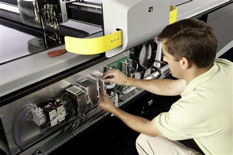
Collaborating With PCB Fabricators Effectively
Effective collaboration with PCB manufacturing companies begins with clear communication of design intent and technical requirements. Before submitting files, confirm their preferred format—whether RS-274X/X2, ODB++, or IPC-2581—to avoid misinterpretations that delay production. Many fabricators provide detailed design guidelines covering trace widths, annular ring sizes, and material specifications; aligning with these early reduces PCB manufacturing cost by minimizing rework.
Proactively discuss critical parameters like layer stackups, impedance control, and finish options. For example, specifying ENIG versus HASL affects both performance and PCB manufacturing business timelines. Use shared checklists or pre-production reviews to verify that your Gerber files match their capabilities. If discrepancies arise, prioritize resolving them through iterative feedback rather than assumptions.
Cost optimization often hinges on balancing design complexity with fabrication realities. Simplify panelization where possible, and clarify tolerances for non-standard features. Leverage your fabricator’s expertise in material substitutions or process adjustments to meet budgetary constraints without sacrificing quality. By treating them as partners rather than vendors, you foster relationships that streamline PCB manufacturing outcomes and build trust for future projects.
ODB vs IPC-2581: Format Selection Tips
When selecting between ODB++ and IPC-2581 for PCB manufacturing, consider the data richness and compatibility each format offers. ODB++, widely adopted by PCB manufacturing companies, excels in conveying layer stackups, netlists, and material specifications in a single package. Its hierarchical structure minimizes file fragmentation, reducing errors during fabrication. However, its reliance on proprietary extensions can sometimes create compatibility hurdles with older CAM tools.
By contrast, IPC-2581 is an open-source standard that integrates design and manufacturing data more cohesively, including impedance requirements and finish tolerances. This makes it ideal for complex projects where PCB manufacturing cost optimization depends on precise, automated data exchange. While newer fabrication facilities increasingly support IPC-2581, verify with your partner whether their systems are updated to parse its XML-based structure.
For PCB manufacturing business stakeholders, the choice often hinges on collaboration depth. If your fabricator prioritizes ODB++, ensure their CAM software aligns with your design tools to avoid rework. Conversely, adopting IPC-2581 future-proofs your workflow but may require upfront training. Always share a test file to validate compatibility before finalizing production—this step prevents delays and ensures both formats meet the manufacturing-ready criteria critical for success.
Ensuring Manufacturing-Ready Gerber Files
To avoid costly delays in PCB manufacturing, start by verifying that your Gerber files meet the exact specifications of your chosen PCB manufacturing companies. Confirm that all layers (copper, solder mask, silkscreen, and drill files) are properly named, aligned, and free of overlapping elements. Use RS-274X or ODB++ formats to ensure compatibility with modern fabrication equipment, as outdated formats may trigger errors or require manual adjustments.
Always cross-check drill files (Excellon format) against your design’s hole sizes and locations—mismatches here can escalate PCB manufacturing cost due to scrap or rework. Include a readme file detailing layer assignments, special tolerances, and surface finish preferences to eliminate guesswork. Tools like Gerber viewers or DFM (Design for Manufacturing) software can flag issues like slivers, acid traps, or insufficient clearances before submission.
Collaborate early with fabricators to validate stack-up requirements and material choices. Many PCB manufacturing business partners offer pre-production reviews to identify discrepancies in annular rings, via tenting, or impedance controls. By prioritizing clarity and precision in your Gerber deliverables, you streamline the entire workflow, reducing risks and ensuring your design transitions seamlessly from prototype to mass production.
Gerber File Validation & Testing Protocols
Before sending files to PCB manufacturing companies, rigorous validation ensures your design aligns with fabrication capabilities. Start by running design rule checks (DRC) to flag issues like trace spacing violations or missing solder masks. Use PCB manufacturing-specific tools like CAM software to simulate how your Gerber files (RS-274X/X2, ODB++, or IPC-2581) will translate into physical layers. Cross-verify drill files against your Gerber layers to prevent mismatches in hole sizes or placements—a common oversight that escalates PCB manufacturing cost.
Collaborate early with your fabricator to confirm their testing protocols. Many PCB manufacturing businesses require aperture lists and stack-up diagrams for precise alignment. Automated optical inspection (AOI) simulations can further identify potential defects, such as copper slivers or annular ring errors, before production. Always validate file integrity by opening them in a viewer like GerberLogix or GC-Prevue to ensure layers render correctly.
Finally, perform a design-for-manufacturability (DFM) analysis to balance performance with producibility. Overlooking this step risks delays, as even minor errors in pad sizes or silkscreen alignment can halt production. By integrating these validation steps, you streamline communication with PCB manufacturing partners and reduce costly revisions.

PCB Drill File Preparation Essentials
When preparing drill files for PCB manufacturing, precision is non-negotiable. Drill files define the location, size, and type of holes required for vias, through-holes, and mounting points, directly impacting the functionality of the final board. Start by ensuring your design software exports Excellon (Format 1 or 2) files with correct tool codes and units—mismatched units between drill files and Gerber layers are a leading cause of fabrication errors.
Collaborate early with PCB manufacturing companies to confirm their tooling capabilities. For instance, specify hole tolerances (e.g., ±3 mil) and aspect ratios to avoid drill bit breakage or incomplete plating. Double-check that non-plated and plated holes are clearly differentiated in your files, as mislabeling can lead to costly rework. Additionally, include a drill legend table in your documentation to help fabricators cross-verify hole sizes against your design intent.
Optimizing drill files also plays a role in managing PCB manufacturing cost. Overly tight tolerances or excessive hole counts can inflate expenses, while redundant tool changes slow production. Use modern CAM tools to merge identical drill sizes and eliminate overlaps. Finally, validate files using DFM checks to flag issues like drill-to-copper clearance violations. By refining these details, you streamline the PCB manufacturing business workflow, reducing delays and ensuring your design transitions seamlessly from prototype to mass production.
Avoiding Common Gerber File Mistakes
Even minor errors in Gerber files can derail PCB manufacturing timelines and inflate PCB manufacturing cost. To prevent setbacks, start by verifying layer alignment and polarity settings. Misaligned copper layers or flipped solder masks often result from overlooked design rule checks (DRCs). Always confirm that aperture definitions match your CAD tool’s output, as mismatches can lead to undefined traces or pads.
Another frequent pitfall is omitting critical layers like drill files or silkscreen markings. Double-check that drill files (Excellon format) include tool sizes and plating specifications, as incomplete data forces PCB manufacturing companies to halt production for clarification. Similarly, ensure all non-functional pads are removed from inner layers to avoid unintended shorts—a common oversight in multilayer designs.
When collaborating with PCB manufacturing business partners, share a readme file detailing layer names, stackup requirements, and special instructions. This reduces back-and-forth and aligns expectations. Finally, avoid using outdated formats like RS-274D; modern PCB manufacturing workflows rely on RS-274X/X2 or ODB++ for embedded attributes. By auditing these details upfront, you sidestep costly revisions and maintain seamless progress from design to fabrication.
Conclusion
Adhering to Gerber fabrication best practices ensures your designs transition seamlessly from concept to physical boards, minimizing errors that could escalate PCB manufacturing cost or delay timelines. By prioritizing file validation and format compliance (RS-274X/X2, ODB++, or IPC-2581), you equip PCB manufacturing companies with precise data to execute your vision accurately. Proactive collaboration with fabricators—clarifying tolerances, material specs, and layer stack-ups—eliminates ambiguities that often derail production.
Remember, even minor oversights in drill file preparation or layer alignment can lead to costly rework, directly impacting the profitability of your PCB manufacturing business. Leverage automated verification tools to cross-check apertures, copper clearances, and solder mask definitions before final submission. This disciplined approach not only streamlines workflows but also builds trust with partners, positioning your projects for repeatable success in a competitive industry.
Ultimately, mastering these protocols transforms PCB manufacturing from a technical hurdle into a strategic advantage, ensuring your designs meet both functional and economic goals without compromise.
Frequently Asked Questions
How do Gerber file formats impact PCB manufacturing costs?
Using optimized formats like RS-274X/X2 or IPC-2581 reduces errors and rework, directly lowering PCB manufacturing costs. Ensure your design software exports these formats to avoid compatibility issues with PCB manufacturing companies.
What should I verify with PCB manufacturing companies before finalizing files?
Confirm their specific requirements for drill files, layer stack-ups, and finish specifications. Misaligned expectations can delay production or increase PCB manufacturing business overhead. Always share a readme file with fabrication notes.
Why do some fabricators prefer ODB++ over Gerber files?
ODB++ bundles design data (drills, layers, netlists) into a single package, streamlining communication. This minimizes back-and-forth with PCB manufacturing partners, especially for complex designs.
How can I avoid common mistakes that increase PCB manufacturing cost?
Double-check copper-to-edge clearances, missing apertures, and polarity mismatches. Run automated validation tools to flag issues early. Collaborate with your PCB manufacturing business partner to review files pre-production.
What role do drill files play in PCB manufacturing success?
Accurate drill files (Excellon format) ensure hole placements match design intent. Errors here lead to misaligned vias or components, risking entire batches. Always include tooling holes and verify units (metric/imperial).
Need Expert Support for Your Project?
For tailored guidance on optimizing files for PCB manufacturing companies, please click here to connect with industry specialists. Streamline your workflow and reduce PCB manufacturing cost with proven strategies.