Gerber File Essentials for Reliable PCB Manufacturing
Key Takeaways
When preparing Gerber files for PCB manufacturing, understanding core principles ensures your design aligns with industry standards. First and foremost, accurate layer configuration prevents miscommunication with PCB manufacturing companies, reducing delays and PCB manufacturing cost. A single missing copper layer or mislabeled drill file can lead to costly revisions, directly impacting your PCB manufacturing business timeline.
Tip: Always cross-verify layer naming conventions (e.g., .GTL for top copper, .GBL for bottom) to avoid fabrication mismatches.
Here’s a quick reference table for critical Gerber components:
| Aspect | Best Practice |
|---|---|
| Layer Configuration | Separate copper, solder mask, and silkscreen layers |
| Formatting Standards | Use RS-274X for embedded apertures |
| Common Errors | Overlooked drill files or mismatched units |
Prioritize design intent clarity by including a README file detailing layer purposes and special requirements. Tools like CAM350 help validate files before submission, ensuring compatibility with manufacturers’ equipment. If you’re optimizing for PCB manufacturing cost, streamline layers by eliminating redundant annotations or unnecessary via configurations.
Remember that tolerances (e.g., trace spacing, annular rings) must align with your manufacturer’s capabilities. By adhering to these practices, you minimize risks in PCB manufacturing workflows, fostering trust and reliability in partnerships with PCB manufacturing companies.

Gerber File Basics for PCB Production
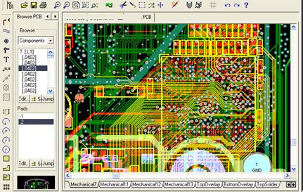
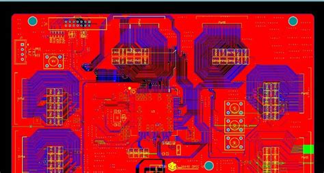
When preparing files for PCB manufacturing, understanding Gerber formats is critical for communicating your design intent accurately. These files act as the universal language between designers and PCB manufacturing companies, detailing every copper trace, solder mask, and drill hole. You’ll typically generate separate Gerber layers for each aspect of your board—such as top/bottom copper, silkscreen, and drill data—ensuring fabricators can replicate your design without ambiguity.
A common pitfall involves mismatched layer assignments, which can escalate PCB manufacturing cost due to rework. Always verify that your layer stack-up aligns with the manufacturer’s specifications. For instance, a four-layer board requires distinct files for inner planes and signal layers, labeled clearly to avoid confusion. Tools like Gerber viewers let you preview how layers interact, catching errors like overlapping pads or missing apertures before submission.
Adhering to RS-274X standards ensures compatibility across most PCB manufacturing business workflows. This format embeds aperture definitions directly into files, eliminating dependencies on external tool lists. Double-check units (metric/imperial) and coordinate precision—even minor discrepancies in decimal places can derail production. By mastering these fundamentals, you streamline communication with fabricators, reducing delays and ensuring your design transitions seamlessly from concept to functional PCB.
Ensuring Manufacturing Reliability Through Gerber Standards
Adhering to Gerber standards ensures your design intent translates accurately into physical boards, minimizing miscommunication with PCB manufacturing companies. Layer mapping errors or ambiguous file formats often lead to costly revisions, directly impacting PCB manufacturing cost and timelines. When you maintain RS-274X compliance, fabrication teams receive unambiguous data for copper layers, solder masks, and silkscreens, reducing the risk of misinterpretation.
Proper aperture definitions and zero-width vector fills eliminate gaps in traces or pads, critical for high-density designs where even micron-level discrepancies can compromise functionality. For instance, omitting drill files or mismatching layer sequences forces manufacturers to guess your requirements, introducing avoidable delays in the PCB manufacturing business. By validating your Gerber outputs with automated DFM checks, you preempt issues like annular ring violations or insufficient clearances before they reach production.
Transitioning between design and fabrication becomes seamless when you align with industry-wide Gerber formatting norms. This precision not only streamlines workflows but also builds trust with partners, ensuring your boards meet reliability benchmarks consistently. Whether optimizing for rapid prototyping or large-scale runs, standardized files act as a universal language across the PCB manufacturing ecosystem.
Step-by-Step Gerber Creation Guide for Error-Free PCBs
Creating Gerber files that meet PCB manufacturing requirements begins with exporting design data from your CAD software. Start by verifying layer assignments—double-check that copper, solder mask, silkscreen, and drill layers align with your PCB manufacturing company‘s specifications. Use standardized naming conventions (e.g., .GTL for top copper) to avoid confusion during fabrication.
Next, configure aperture lists and ensure all shapes (pads, traces, vias) adhere to your fabricator’s PCB manufacturing cost-optimized design rules. Missing or mismatched apertures can lead to misinterpretation, delaying production. Export each layer separately, confirming non-plated through-holes (NPTH) and plated through-holes (PTH) are clearly differentiated in drill files.
After exporting, run a Design Rule Check (DRC) to flag overlaps, spacing violations, or missing layers. Many PCB manufacturing businesses reject files with unresolved DRC errors, as these often cause short circuits or open connections. Validate your Gerber set using free viewers like Gerbv or commercial tools to simulate how manufacturers will interpret the data.
Finally, compress all files into a single ZIP folder and include a readme.txt with layer descriptions, stackup details, and special instructions. This step minimizes back-and-forth communication, ensuring your design aligns with the fabricator’s workflow. By following this structured approach, you reduce risks of costly revisions and maintain seamless collaboration with PCB manufacturing partners.
Common PCB Design Mistakes in Gerber File Preparation
When preparing Gerber files for PCB manufacturing, even minor oversights can lead to costly delays or fabrication errors. One common mistake is neglecting to include all critical layers in the export settings, such as solder mask or silkscreen layers, which forces PCB manufacturing companies to request revisions. Another frequent oversight involves mismatched aperture definitions, where shapes in the design don’t align with the tools used by fabricators—a problem that inflates PCB manufacturing cost due to manual corrections.
Designers often forget to verify clearance tolerances between copper traces and board edges, risking short circuits during panelization. Similarly, improper layer naming or stacking order confuses fabrication teams, especially when working with complex multilayer designs. These errors disrupt PCB manufacturing business workflows, as engineers spend hours reconciling ambiguous files instead of focusing on production.
To avoid these pitfalls, always cross-check your Gerber files against industry standards like IPC-2581 or RS-274X. Use automated DFM (Design for Manufacturability) checks to flag issues like overlapping pads or missing drill files. By addressing these details upfront, you ensure smoother communication with manufacturers and reduce the risk of costly re-spins. Remember: precision in Gerber file preparation isn’t just about compliance—it’s about building trust with partners across the PCB manufacturing supply chain.
Gerber Formatting Standards for Seamless Fabrication
Adhering to Gerber formatting standards ensures your design translates accurately into physical boards during PCB manufacturing. Most PCB manufacturing companies rely on RS-274X (Extended Gerber) as the industry benchmark, which supports embedded apertures and layer-specific data. Critical elements like solder mask layers, copper traces, and drill files must follow precise naming conventions (e.g., .GTL for top layer, .GBL for bottom layer) to avoid misinterpretation. Misaligned apertures, overlapping geometries, or missing polarity indicators can trigger fabrication errors, increasing PCB manufacturing cost due to rework delays.
To streamline workflows, verify that your design software exports files with 1:1 scaling and absolute coordinates. Avoid using non-standard file extensions or custom layer labels, as these confuse automated systems in the PCB manufacturing business. Double-check aperture lists for consistency—mismatched tool definitions lead to undersized holes or incomplete etching. By validating your Gerber files against IPC-2581 or manufacturer-specific design rules, you preempt costly revisions and maintain alignment with global fabrication standards. This disciplined approach minimizes production bottlenecks, ensuring your boards meet both technical specifications and delivery timelines.
Layer Configuration Best Practices in Gerber Files
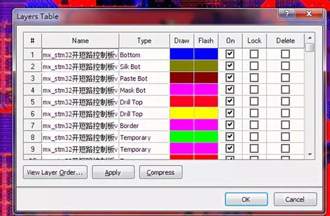
When configuring layers in Gerber files, precision ensures PCB manufacturing companies can interpret designs without ambiguity. Start by defining layer purposes clearly—label copper layers (e.g., Top Layer, Inner1), solder mask, silkscreen, and drill files with standardized naming conventions. Mislabeled layers often lead to delays, increasing PCB manufacturing cost due to rework. For multi-layer boards, confirm the stacking order matches fabrication requirements, as errors here risk board functionality.
Use Gerber extensions (e.g., .GTL for top layer, .GBL for bottom layer) to align with industry norms. Include all critical layers, even if unused, to avoid incomplete data submissions. For instance, omitting drill files (.TXT or .DRL*) forces fabricators to guess hole placements, jeopardizing alignment. If your design includes non-standard features like blind vias, annotate these explicitly in layer notes to streamline communication with PCB manufacturing business partners.
Finally, validate layer visibility and polarity settings. Solder mask layers should specify openings (positive polarity) rather than covered areas to prevent misinterpretation. By adhering to these practices, you reduce prototyping cycles and ensure PCB manufacturing workflows remain efficient, minimizing both time and cost overheads.
Streamlining PCB Workflows via Gerber File Optimization
Optimizing Gerber files is critical for reducing delays and minimizing PCB manufacturing cost while maintaining quality. By adopting standardized design-to-production practices, you ensure that PCB manufacturing companies can interpret your files accurately, avoiding costly revisions. Start by organizing layers logically—labeling copper, solder mask, and silkscreen layers clearly helps fabricators align materials correctly. Use unified naming conventions (e.g., “TOP_COPPER” or “BOTTOM_SOLDERMASK”) to eliminate ambiguity, which is especially vital when collaborating with global PCB manufacturing business partners.
Automated design rule checks (DRCs) streamline workflows by flagging issues like incomplete apertures or mismatched layer pairs before files are exported. This proactive approach reduces back-and-forth communication, accelerating timelines. For instance, embedding drill files (Excellon format) alongside Gerber layers ensures precise hole alignment, a common pain point in PCB manufacturing. Tools like DFM analysis software further refine files by simulating fabrication outcomes, letting you adjust tolerances or pad sizes early.
Finally, version control systems prevent file mismatches during iterative design updates. When every hour saved translates to lower PCB manufacturing cost, these optimizations directly impact your project’s bottom line. By prioritizing clarity and consistency, you empower PCB manufacturing companies to focus on quality rather than troubleshooting errors—turning streamlined workflows into competitive advantages.

Troubleshooting Gerber Errors for Manufacturing Success
Even minor Gerber file errors can derail PCB manufacturing timelines and inflate PCB manufacturing cost. To avoid costly revisions, start by verifying layer alignment—mismatched copper and solder mask layers are a leading cause of fabrication delays. Use design rule checks (DRC) to flag overlaps, gaps, or missing apertures that PCB manufacturing companies often encounter. If your board house reports inconsistent drill files, cross-check tool sizes and ensure all plated holes are properly annotated.
Another critical step involves validating file formats. Exporting Gerbers in RS-274X (Extended Gerber) ensures compatibility with modern equipment, reducing parsing errors during production. For complex designs, share a readme.txt file detailing layer assignments and special requirements—this minimizes back-and-forth communication with your PCB manufacturing business partner.
When troubleshooting, simulate fabrication workflows using Gerber viewers like GC-Prevue or ViewMate. These tools reveal hidden issues, such as silkscreen encroaching on pads or soldermask clearance errors, which might escape CAD software checks. Proactively addressing these flaws not only accelerates approvals but also strengthens trust with PCB manufacturing providers. Remember, every unresolved error translates to wasted materials and labor—factors that directly impact your project’s bottom line. By refining these practices, you create a seamless bridge between design intent and manufacturable reality.
Conclusion
When preparing Gerber files for PCB manufacturing, attention to detail ensures seamless collaboration with PCB manufacturing companies. By adhering to standardized formatting and layer configuration practices, you minimize errors that could escalate PCB manufacturing cost or delay timelines. Precision in file creation not only streamlines workflows but also builds trust with fabrication partners, critical for sustaining a competitive PCB manufacturing business.
Always validate your designs against industry standards like RS-274X and cross-check layer assignments to avoid misinterpretation. Tools such as Gerber viewers and DFM analysis software act as safeguards, catching discrepancies before they reach production. Remember, even minor oversights—like missing solder mask layers or misaligned drill files—can lead to costly revisions.
Ultimately, the reliability of your PCB hinges on how effectively you translate design intent into Gerber data. By prioritizing error-free outputs and maintaining open communication with manufacturers, you ensure your files meet both technical and commercial expectations. This disciplined approach not only accelerates prototyping but also strengthens your position in a market where PCB manufacturing efficiency directly impacts project success.
FAQs
How do Gerber files impact pcb manufacturing reliability?
Gerber files serve as the universal language between designers and pcb manufacturing companies. Incorrect layer mapping or missing files can lead to production delays, directly affecting pcb manufacturing cost and timelines. Always verify layer labels and aperture lists before submission.
What common errors increase pcb manufacturing cost?
Overlooking design rule checks (DRC) or using non-standard drill files often forces manufacturers to request revisions. For example, mismatched solder mask layers may require reprocessing, inflating pcb manufacturing business expenses. Use automated validation tools to catch these issues early.
Can improper layer configuration delay production?
Yes. Misaligned copper layers or undefined board outlines create ambiguity during fabrication. Most pcb manufacturing companies require clear layer stacking details to avoid misinterpretation. Reference IPC-2581 or RS-274X standards to ensure compatibility.
How do Gerber files streamline workflows for startups?
Accurate Gerber data reduces back-and-forth communication, allowing pcb manufacturing partners to prioritize your order. Startups focusing on pcb manufacturing cost optimization benefit from error-free files that minimize scrap rates and rework fees.
Why do some manufacturers reject Gerber files?
Issues like missing drill tables, unassigned layers, or incompatible formats (e.g., non-extended Gerber) are common rejection reasons. Partner with pcb manufacturing business experts who offer pre-production file reviews to mitigate risks.
Ready to Optimize Your PCB Production?
For tailored guidance on Gerber file preparation and pcb manufacturing cost strategies, please click here to connect with industry-certified specialists.