The Comprehensive Guide to BGA PCB: Design, Manufacturing, and Assembly
Introduction to BGA PCB Technology
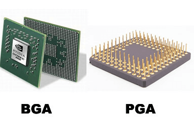
Ball Grid Array (BGA) printed circuit boards represent one of the most significant advancements in electronic packaging technology. As integrated circuits continue to increase in complexity and pin count, traditional packaging methods like quad flat packages (QFP) have become limiting factors in electronic design. BGA technology emerged as a solution to these challenges, offering higher density interconnections, improved thermal performance, and enhanced electrical characteristics.
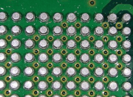
The fundamental concept of BGA packaging involves mounting the integrated circuit on the bottom side of the package with an array of solder balls that serve as both electrical connections and mechanical attachments to the PCB. This configuration provides several advantages over peripheral-lead packages, including reduced package size, shorter interconnection paths, and better heat dissipation capabilities.
BGA Package Types and Variations
The BGA family encompasses several specialized package types, each designed to address specific application requirements:
- Plastic BGA (PBGA): The most common and cost-effective BGA variant, using a plastic substrate material. PBGAs typically offer good thermal and electrical performance for mainstream applications.
- Ceramic BGA (CBGA): Featuring a ceramic substrate, these packages provide superior thermal conductivity and mechanical stability, making them ideal for high-reliability applications in aerospace, military, and medical fields.
- Metal BGA (MBGA): Incorporating metal layers for enhanced thermal management, MBGAs are particularly suited for high-power applications where heat dissipation is critical.
- Tape BGA (TBGA): Utilizing a flexible tape substrate, TBGAs offer a thin profile solution for space-constrained applications while maintaining good electrical performance.
- Flip Chip BGA (FCBGA): This advanced configuration eliminates the need for wire bonds by flipping the die and connecting it directly to the substrate through solder bumps, resulting in superior electrical performance.
- Chip-Scale BGA (CSBGA): With a package size barely larger than the silicon die itself, CSBGAs represent the ultimate in miniaturization for portable and compact devices.
- Stacked BGA: These innovative packages incorporate multiple dies stacked vertically within a single package, dramatically increasing functionality while conserving board space.
BGA PCB Design Considerations
Designing printed circuit boards for BGA components requires careful attention to numerous factors to ensure reliability and performance:
Pad Design and Layout
The foundation of successful BGA implementation lies in proper pad design. Key considerations include:
- Pad size relative to solder ball diameter (typically 80-90% of ball diameter)
- Pad shape (circular vs. square)
- Solder mask definition (solder mask defined vs. non-solder mask defined pads)
- Pad finish selection (ENIG, OSP, immersion silver, etc.)
Routing Strategies
BGA escape routing presents unique challenges due to the high density of connections:
- Layer count determination based on pin count and pitch
- Via selection (through-hole, blind, buried, or microvia)
- Fanout patterns (dog-bone, via-in-pad, or direct pad routing)
- Trace width and spacing considerations
Thermal Management
Effective heat dissipation is critical for BGA packages:
- Thermal via arrays under high-power devices
- Copper balancing to prevent warpage
- Heat spreader incorporation
- Consideration of thermal interface materials
Signal Integrity
Maintaining signal quality in BGA designs requires:
- Proper power delivery network design
- Impedance control for high-speed signals
- Crosstalk mitigation techniques
- Length matching for differential pairs
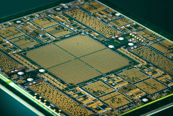
BGA PCB Manufacturing Processes
The production of BGA-compatible PCBs demands specialized manufacturing processes to meet the tight tolerances required:
Substrate Fabrication
- High-precision drilling for microvias (laser drilling for HDI boards)
- Sequential lamination for multilayer boards
- Tight control of dielectric thicknesses
- Advanced plating processes for via filling
Surface Finishes
The choice of surface finish significantly impacts BGA assembly yield:
- Electroless Nickel Immersion Gold (ENIG): The most common BGA finish
- Organic Solderability Preservative (OSP): Cost-effective but less durable
- Immersion Silver: Good performance with some tarnishing concerns
- Electroless Nickel Electroless Palladium Immersion Gold (ENEPIG): High-end solution
- Immersion Tin: Economical but with limited shelf life
Solder Mask Application
- Liquid Photoimageable Solder Mask (LPSM) or Dry Film Solder Mask
- Precise registration requirements
- Optimal thickness control
- Proper opening geometry for BGA pads
BGA Assembly Techniques
The assembly process for BGAs requires specialized equipment and processes:
Solder Paste Printing
- Stencil design considerations (thickness, aperture size, and geometry)
- Solder paste selection (particle size, alloy composition, flux chemistry)
- Printing parameter optimization (pressure, speed, separation)
Component Placement
- High-precision placement machines with vision systems
- Warpage compensation for large BGAs
- Placement force control to prevent damage
Reflow Soldering
- Thermal profile development considering package mass
- Ramp rates and peak temperature control
- Time above liquidus (TAL) optimization
- Nitrogen atmosphere considerations
Inspection and Testing
- X-ray inspection for solder joint evaluation
- Automated Optical Inspection (AOI) for surface defects
- Boundary scan testing for electrical verification
- Functional testing under thermal stress
Rework and Repair of BGA Assemblies
Despite best efforts in design and manufacturing, BGA rework is sometimes necessary:
Removal Techniques
- Dedicated BGA rework stations with bottom heating
- Thermocouple placement for temperature monitoring
- Proper shielding of adjacent components
Site Preparation
- Solder removal using desoldering braid or vacuum tools
- Pad cleaning and inspection
- Surface finish restoration if needed
Reballing and Reattachment
- Solder ball placement methods (preforms, stencil printing, or syringe dispensing)
- Flux application techniques
- Reflow profile optimization for rework
Reliability Considerations for BGA PCBs
Ensuring long-term reliability of BGA assemblies involves addressing several potential failure mechanisms:
Thermal Cycling Performance
- Coefficient of Thermal Expansion (CTE) matching
- Solder joint fatigue analysis
- Accelerated life testing methodologies
Mechanical Stress
- Board flexure effects
- Shock and vibration resistance
- Underfill material selection and application
Electromigration
- Current density analysis
- Intermetallic compound formation
- Kirkendall voiding prevention
Moisture Sensitivity
- MSL (Moisture Sensitivity Level) classification
- Proper handling and baking procedures
- Popcorning prevention during reflow
Advanced BGA Technologies
The evolution of BGA packaging continues with several cutting-edge developments:
3D Packaging
- Package-on-package (PoP) configurations
- Through-silicon vias (TSVs) for vertical integration
- Silicon interposer technology
High-Density Interconnect (HDI)
- Microvia-in-pad technology
- Sequential build-up layers
- Any-layer via structures
Embedded Components
- Passive components within the PCB substrate
- Active die embedding techniques
- Thermal management solutions for embedded devices
Future Trends in BGA PCB Technology
The BGA landscape continues to evolve with several emerging trends:
Fine-Pitch BGAs
- Pitch reduction below 0.5mm
- Advanced assembly techniques for ultra-fine pitch
- Mixed pitch designs within single packages
High-Speed Designs
- Signal integrity optimization for multi-gigabit interfaces
- Low-loss material adoption
- Advanced power delivery networks
Heterogeneous Integration
- Combining disparate technologies in single packages
- Chiplet-based architectures
- Advanced thermal management solutions
Sustainable Manufacturing
- Lead-free and halogen-free material development
- Energy-efficient production processes
- Recycling and reuse strategies
Conclusion
BGA PCB technology has become indispensable in modern electronics, enabling the continued advancement of device miniaturization and performance. From consumer electronics to aerospace applications, BGAs provide the interconnection density and reliability required by today’s complex systems. Successful implementation requires careful consideration of design rules, material selection, manufacturing processes, and assembly techniques. As the technology continues to evolve with finer pitches, 3D integration, and advanced materials, BGA packages will remain at the forefront of electronic packaging solutions, driving innovation across all sectors of the electronics industry.
Designers and manufacturers must stay abreast of these developments while maintaining rigorous quality standards to ensure the reliability of BGA assemblies. With proper implementation, BGA technology offers an unparalleled combination of performance, density, and manufacturability that will continue to power electronic innovation for years to come.