Advanced PCB Manufacturing and Assembly Best Practices
Key Takeaways
Effective PCB assembly relies on harmonizing design, material, and process innovations. Central to this is integrating design for manufacturability (DFM) principles early in development to minimize errors and reduce costs. Prioritizing high-performance substrates—such as FR-4, polyimide, or ceramic-filled laminates—ensures thermal stability and signal integrity, particularly in demanding environments.
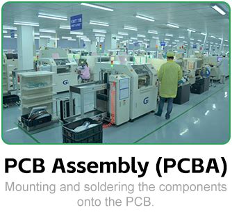
Automation remains pivotal in modern PCBA workflows, with robotic soldering and pick-and-place systems achieving micron-level accuracy while accelerating throughput. Complementing this, advanced inspection tools like automated optical inspection (AOI) and X-ray testing enforce rigorous quality control, catching defects before final integration.
| Traditional Approach | Advanced Technique |
|---|---|
| Manual component placement | Robotic pick-and-place systems |
| Visual inspection | AOI and X-ray validation |
| Trial-and-error prototyping | Simulation-driven DFM checks |
Streamlining production further demands adherence to industry-standard protocols, such as IPC-A-610 and ISO 9001, which govern assembly tolerances and documentation. By balancing material compatibility with automated precision, manufacturers achieve repeatable outcomes while scaling operations efficiently. These strategies collectively ensure PCB assembly aligns with evolving technological and regulatory demands.
Optimizing PCB Design for Efficient Manufacturing
Effective PCB assembly begins with design decisions that account for manufacturability. Proper component placement, spacing, and routing directly influence yield rates and PCBA reliability. Design for Manufacturability (DFM) principles recommend maintaining adequate clearance between high-density components to prevent solder bridging during reflow processes. Additionally, aligning pad sizes with component leads ensures consistent solder joint formation.
Tip: Follow IPC-2221A guidelines for trace width and spacing to minimize impedance mismatches and signal loss in high-frequency circuits.
Incorporating automated optical inspection (AOI)-friendly features, such as fiducial markers and test points, streamlines post-assembly quality checks. Designers should also prioritize thermal management by balancing copper distribution and avoiding localized hotspots. For multilayer boards, symmetry in stack-up configuration reduces warpage risks during lamination.
Transitioning to panelized designs with standardized breakaway tabs can optimize material usage and reduce waste. When integrating mixed-technology components (e.g., through-hole and surface-mount), group similar parts to minimize machine recalibration during PCB assembly. Finally, verifying designs against manufacturer-specific capabilities—such as minimum drill sizes or solder mask tolerances—ensures compatibility with PCBA workflows.
Selecting High-Performance PCB Materials
The foundation of reliable PCB assembly lies in strategic material selection, which directly impacts electrical performance, thermal management, and long-term durability. High-frequency applications, for instance, demand substrates with low dielectric loss, such as Rogers RO4000® or PTFE-based laminates, to minimize signal distortion. Conversely, industrial-grade PCBA often prioritizes thermal stability, favoring materials like FR-4 TG170 or polyimide for their resistance to extreme temperatures and mechanical stress.
When evaluating materials, consider coefficient of thermal expansion (CTE) compatibility between layers to prevent delamination during thermal cycling. For high-power designs, metal-core substrates (e.g., aluminum-backed PCBs) enhance heat dissipation, while ceramic-filled laminates improve insulation properties. Surface finishes like ENIG (Electroless Nickel Immersion Gold) or OSP (Organic Solderability Preservative) further influence solderability and corrosion resistance in PCB assembly workflows.
Advanced PCBA projects increasingly integrate high-speed digital materials such as Megtron 6 or Isola I-Speed, which balance signal integrity with cost efficiency. Collaboration between design engineers and manufacturers is critical to align material choices with automated assembly processes, ensuring compatibility with pick-and-place machinery and reflow soldering profiles. By prioritizing material properties that align with operational demands and industry-standard protocols, manufacturers can mitigate risks and optimize performance across the product lifecycle.
Automating Assembly Processes for Precision
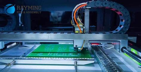
Modern PCB assembly workflows increasingly rely on automation to achieve micron-level accuracy and repeatability. By integrating robotic pick-and-place systems with vision-guided alignment, PCBA (printed circuit board assembly) lines can position components as small as 01005 packages with tolerances under ±25μm. This precision minimizes human error, particularly in high-density designs requiring fine-pitch BGAs or microvia interconnects. Automated optical inspection (AOI) systems further enhance reliability by scanning solder joints and component orientations in real time, flagging deviations before boards advance to reflow ovens.
Advanced PCB assembly platforms now combine surface-mount technology (SMT) with AI-driven process optimization. For example, closed-loop feedback mechanisms adjust stencil pressure or solder paste volume dynamically, ensuring consistent deposition across varying board geometries. Such automation not only accelerates throughput but also supports mixed-technology assemblies—blending through-hole and SMT components—without compromising placement accuracy.
To maintain alignment with industry benchmarks, manufacturers are adopting Industry 4.0 principles, where PCBA equipment shares data with enterprise resource planning (ERP) systems. This connectivity enables predictive maintenance, reducing downtime, and ensures traceability for compliance with aerospace or medical-grade standards. As automation evolves, its role in balancing speed, precision, and scalability will remain critical for next-generation electronics manufacturing.
Implementing Rigorous Quality Control Standards
Effective PCB assembly relies on systematic quality control frameworks that address defects at every production stage. Modern pcb assembly workflows integrate Automated Optical Inspection (AOI) and X-ray testing to detect solder joint irregularities, component misalignment, or micro-cracks in high-density PCBA units. By enforcing IPC-A-610 and IPC-J-STD-001 standards, manufacturers ensure solderability, cleanliness, and mechanical integrity across multilayer boards.
Critical checkpoints include incoming material verification to validate substrate quality and copper thickness, followed by in-process inspections during solder paste application and reflow profiling. Post-assembly, functional testing simulates real-world operating conditions, while environmental stress screening (ESS) identifies latent failures in PCBA under thermal or vibrational loads. Implementing statistical process control (SPC) tools further minimizes variability by monitoring key parameters like line impedance and signal integrity.
To maintain compliance, cross-functional teams audit documentation trails, from Bill of Materials (BOM) accuracy to revision-controlled design files. This proactive approach not only reduces rework costs but also aligns with ISO 9001 and IATF 16949 certifications, essential for automotive or aerospace applications. By embedding quality assurance into PCB assembly workflows, manufacturers achieve consistent yield rates while meeting evolving industry benchmarks.
Streamlining Production With Advanced Techniques
Modern PCB assembly workflows achieve peak efficiency by strategically implementing automation and digital integration. Robotic pick-and-place systems combined with AI-driven optical inspection tools minimize human error while accelerating PCBA processes. Factories leveraging Industrial Internet of Things (IIoT) platforms can monitor production lines in real time, enabling dynamic adjustments to optimize throughput. Automated storage and retrieval systems (AS/RS) ensure precise material handling, reducing component misplacement by up to 40% in high-volume runs.
Embedding design for manufacturability (DFM) checks within the engineering phase prevents costly revisions, with simulation software identifying potential assembly conflicts before prototyping. This proactive approach shortens PCBA development cycles by 25–30%, according to industry benchmarks. Advanced soldering techniques like laser reflow further enhance consistency, particularly for miniaturized components in IoT devices.
By synchronizing these innovations, manufacturers achieve a 15–20% reduction in per-unit costs while maintaining IPC-A-610 compliance standards. The integration of machine learning algorithms into quality assurance systems enables predictive maintenance, cutting unplanned downtime by over 50%. These methodologies not only streamline operations but also create scalable frameworks adaptable to evolving PCB assembly requirements across aerospace, medical, and automotive sectors.
Ensuring Precision in PCB Component Assembly
Achieving precision in PCB assembly requires a combination of advanced equipment, process optimization, and meticulous attention to detail. Modern PCBA workflows leverage automated optical inspection (AOI) systems and high-speed pick-and-place machines to ensure components are positioned with micron-level accuracy. These systems minimize human error, particularly when handling miniature or high-density parts like ball grid arrays (BGAs) or 01005 passive components.
Critical to this process is the calibration of soldering parameters, including thermal profiles for reflow ovens, which directly impact joint integrity. Implementing design for manufacturability (DFM) guidelines ensures components are spaced optimally, reducing risks of tombstoning or solder bridging. Additionally, real-time monitoring of stencil printing consistency guarantees even solder paste deposition—a foundational step for reliable electrical connections.
To maintain alignment with industry standards, manufacturers often integrate in-circuit testing (ICT) and functional testing at multiple stages. These checks validate not only placement accuracy but also electrical performance under simulated operating conditions. By combining automated assembly with rigorous validation protocols, PCBA providers can deliver boards that meet both functional specifications and long-term reliability requirements, seamlessly transitioning to downstream quality assurance processes outlined in subsequent sections.
Adopting Industry-Standard PCB Protocols
Adherence to industry-standard protocols is critical for ensuring consistency and reliability in PCB assembly workflows. By aligning with globally recognized frameworks such as IPC-A-610 (Acceptability of Electronic Assemblies) and IPC-J-STD-001 (Requirements for Soldered Electrical Connections), manufacturers establish a baseline for PCBA quality, reducing defects and rework. These standards govern every phase, from solder joint integrity to component placement accuracy, ensuring compliance with automated assembly systems and high-density interconnect (HDI) designs.
Integrating design-for-manufacturability (DFM) checks early in the process further aligns production with these protocols. For instance, verifying pad geometries against IPC-7351 specifications minimizes soldering risks during surface-mount technology (SMT) applications. Additionally, standardized documentation practices—such as Gerber file validation and bill of materials (BOM) cross-referencing—streamline communication between design and PCB assembly teams, mitigating errors before prototyping.
Regular audits and certification renewals, including ISO 9001 and UL certification, reinforce compliance with evolving industry demands. This proactive approach not only optimizes PCBA yields but also strengthens supply chain partnerships, as stakeholders prioritize vendors adhering to unified quality benchmarks. By embedding these protocols into workflows, manufacturers future-proof operations against shifting regulatory landscapes while maintaining alignment with automated precision assembly trends.
Integrating DFM Principles in PCB Creation
Incorporating Design for Manufacturing (DFM) principles early in the PCB assembly process ensures seamless translation of design intent into functional, reliable products. By prioritizing manufacturability, engineers can address potential fabrication challenges—such as component spacing, trace width consistency, and thermal management—before transitioning to PCBA (printed circuit board assembly). For instance, optimizing pad sizes and aligning placement with automated pick-and-place machinery reduces rework rates and accelerates production cycles.
A critical aspect of DFM involves material compatibility analysis, where substrate properties and solder mask specifications are evaluated against thermal and mechanical stresses during PCB assembly. Tools like 3D modeling software and design rule checks (DRCs) enable designers to simulate manufacturing outcomes, identifying areas where adjustments—such as reducing high-density via clusters—can enhance yield rates. Collaboration between design and manufacturing teams further refines tolerances, ensuring alignment with PCBA equipment capabilities.
Adhering to DFM guidelines not only minimizes defects but also lowers costs by streamlining workflows. For example, standardizing layer stack-ups and avoiding non-standard drill sizes simplifies procurement and reduces lead times. By embedding these practices into the design phase, companies achieve a balance between innovation and practicality, fostering scalable solutions that meet evolving industry demands.
Conclusion
In modern electronics production, success in PCB assembly hinges on harmonizing innovative techniques with meticulous execution. By integrating design-for-manufacturing (DFM) principles early in the development cycle, teams can preemptively address potential flaws, reducing costly revisions during PCBA stages. Advanced automation, such as automated optical inspection (AOI) and surface-mount technology (SMT), ensures consistent precision while accelerating throughput—a critical advantage in high-volume manufacturing.
Equally vital is the adherence to industry-standard protocols like IPC Class 3 and ISO 9001, which safeguard reliability across PCB assembly workflows. Rigorous quality control measures, including electrical testing and thermal stress analysis, validate performance under real-world conditions. Furthermore, selecting materials with optimal thermal stability and signal integrity directly impacts the longevity of PCBA outputs, particularly in demanding applications like aerospace or IoT devices.
Ultimately, the convergence of automated processes, robust material science, and data-driven quality frameworks establishes a foundation for scalable, error-resistant production. As technology evolves, manufacturers prioritizing these best practices will not only meet current benchmarks but also adapt seamlessly to emerging standards, securing their position in a competitive global market.
Frequently Asked Questions
What distinguishes PCB assembly from PCBA?
PCB assembly refers to the process of populating a bare circuit board with components, while PCBA (Printed Circuit Board Assembly) denotes the fully assembled and functional unit. The latter includes soldering, testing, and validation stages critical for operational reliability.
How does design optimization influence manufacturing efficiency?
Optimizing designs for PCB assembly reduces material waste and minimizes errors during production. Techniques like panelization and proper component spacing accelerate automated assembly, ensuring compatibility with pick-and-place machines and reflow ovens.
What materials are prioritized for high-frequency applications?
High-performance substrates like Rogers RO4000 or Teflon are preferred for their stable dielectric properties. Material selection directly impacts signal integrity, especially in RF or high-speed digital PCBA applications.
Why is automated optical inspection (AOI) mandatory in quality control?
AOI systems detect soldering defects, misaligned components, and trace anomalies with micron-level precision. This step is vital for maintaining industry standards like IPC-A-610, reducing post-production failures by over 70%.
How do DFM principles streamline production timelines?
Design-for-Manufacturing (DFM) guidelines eliminate ambiguities in fabrication files, ensuring compatibility with automated processes. This reduces engineering queries by 40% and shortens lead times for complex PCB assembly projects.
Ready to Elevate Your PCB Production?
For tailored solutions in PCB assembly and PCBA prototyping, please click here to explore our professional services. Our expertise ensures adherence to ISO 9001 and IPC Class 3 standards for mission-critical applications.