Leading-Edge PCB Assembly Services for Innovative Designs
Key Takeaways
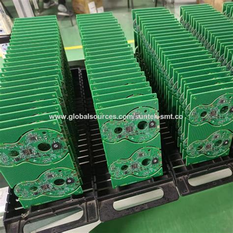
Modern PCB assembly processes are foundational to delivering high-performance electronic devices. By leveraging advanced manufacturing techniques, engineers can achieve micron-level precision in component placement, ensuring reliability for complex designs. PCBA (Printed Circuit Board Assembly) services now integrate automated optical inspection (AOI) and X-ray testing, reducing defects by up to 98% in mission-critical applications.
"Choosing a PCB assembly partner with expertise in rapid prototyping accelerates time-to-market while maintaining design integrity."
| Service Feature | Traditional Methods | Advanced PCBA Solutions |
|---|---|---|
| Turnaround Time | 10–14 days | 3–5 days |
| Error Detection | Manual Inspection | AI-Driven AOI Systems |
| Scalability | Limited Batch Sizes | Flexible, High-Volume Output |
For innovative designs, scalable production strategies enable seamless transitions from prototyping to mass manufacturing. Techniques like surface-mount technology (SMT) and through-hole assembly (THA) are optimized for next-gen devices, balancing thermal management and signal integrity. Additionally, PCB assembly workflows now incorporate eco-friendly materials, aligning with global sustainability standards without compromising performance.
By prioritizing PCBA innovations—such as embedded component technology—engineers can enhance power efficiency and reduce form factors, meeting the demands of IoT, wearables, and AI-driven systems.
Advanced PCB Assembly Techniques for Electronics
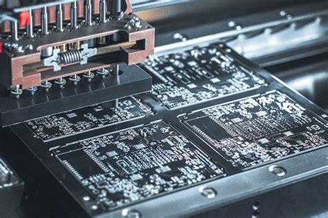
Modern PCB assembly processes have evolved to address the increasing complexity of electronic devices, integrating precision and adaptability at every stage. Central to this advancement is the use of surface-mount technology (SMT), which enables high-density component placement while minimizing board space. Combined with automated optical inspection (AOI), manufacturers ensure near-zero defect rates, critical for applications in aerospace, medical devices, and IoT systems.
A key innovation lies in mixed-technology assembly, merging through-hole components with SMT to optimize reliability in high-stress environments. This hybrid approach supports designs requiring both mechanical durability and miniaturization. Additionally, PCBA workflows now incorporate real-time data analytics, allowing engineers to adjust parameters like solder paste viscosity or reflow temperatures dynamically.
For rapid iteration, laser-direct imaging (LDI) accelerates prototype development by eliminating photomasks, reducing lead times by up to 40%. Such techniques align with scalable production models, ensuring seamless transitions from low-volume batches to mass manufacturing. By prioritizing design for manufacturability (DFM), teams preemptively address potential bottlenecks, balancing performance with cost efficiency.
These advancements underscore how modern PCB assembly techniques are not just enhancing current electronics but redefining what’s possible in next-generation device development.
Precision Engineering in Modern PCB Manufacturing
At the core of modern electronics development lies precision engineering, a discipline that ensures every PCB assembly meets exacting standards for performance and reliability. Advanced PCBA processes now integrate laser-drilled microvias and high-density interconnect (HDI) technology, enabling the creation of ultra-compact circuits without compromising signal integrity. These innovations are critical for applications demanding miniaturization and high-speed operation, such as wearable tech and IoT devices.
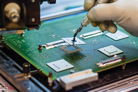
To achieve this level of accuracy, manufacturers employ automated optical inspection (AOI) systems and 3D solder paste inspection (SPI) tools. These technologies detect micron-level defects in real time, ensuring that every PCB assembly aligns with design specifications. Additionally, the use of lead-free soldering and thermal management solutions enhances durability, particularly in harsh environments like automotive or aerospace systems.
By combining precision engineering with scalable PCBA workflows, companies can seamlessly transition from prototyping to mass production. This synergy reduces time-to-market while maintaining consistency across batches—a vital factor for industries requiring both innovation and reliability. As next-gen devices push the boundaries of complexity, the role of advanced manufacturing techniques in PCB assembly will only grow more pivotal.
Rapid Prototyping Solutions for Innovative Designs
In the realm of PCB assembly, accelerating the transition from concept to functional prototype is critical for staying ahead in competitive markets. Modern PCBA workflows leverage automated design validation and high-speed component placement to reduce iteration cycles from weeks to days. By integrating advanced manufacturing techniques like laser-direct imaging and 3D solder paste inspection, engineers can swiftly identify design flaws while maintaining precision engineering standards.
For startups and R&D teams, rapid prototyping bridges the gap between experimental layouts and mass-production-ready designs. Tools such as real-time thermal simulation and flexible substrate testing enable designers to validate performance under extreme conditions before committing to full-scale scalable production. This approach not only minimizes material waste but also ensures compliance with industry-specific certifications like IPC-A-610.
Transitioning seamlessly into high-volume manufacturing requires aligning prototyping phases with next-gen PCB innovation. Partnering with PCBA specialists who offer agile supply chain integration ensures that design optimizations—such as embedded components or mixed-technology boards—are scalable. As a result, businesses can confidently iterate on innovative designs while meeting tight deadlines, ultimately delivering cutting-edge electronics that outperform market expectations.
Scalable Production Strategies for Next-Gen PCBs
Achieving scalability in PCB assembly requires balancing flexibility with standardized processes. Modern PCBA workflows integrate modular manufacturing lines that adapt to varying production volumes, enabling seamless transitions from low-volume prototyping to high-volume output. By leveraging automated pick-and-place systems and AI-driven quality control, manufacturers reduce lead times while maintaining precision—critical for next-gen devices demanding miniaturization and high-density interconnects.
A key strategy involves design-for-manufacturability (DFM) principles, which align product designs with scalable PCB assembly capabilities. This reduces iterative revisions and accelerates time-to-market. Advanced factories also employ demand forecasting tools to optimize inventory management, ensuring components like microcontrollers or high-frequency substrates are available without overstocking.
For industries requiring rapid scaling, cloud-based production monitoring provides real-time insights into PCBA line efficiency, identifying bottlenecks in solder paste application or reflow processes. Pairing this with hybrid manufacturing models—combining in-house expertise with trusted partners—ensures capacity can expand dynamically.
Finally, sustainable scalability hinges on material optimization. Using halogen-free laminates or recyclable substrates not only meets environmental regulations but also future-proofs production lines against supply chain disruptions. By embedding these strategies, businesses unlock the agility needed to meet evolving demands for advanced electronics.
Optimizing Electronics with Cutting-Edge Assembly
Modern electronics demand PCB assembly processes that prioritize both precision and adaptability. By integrating automated optical inspection (AOI) and surface-mount technology (SMT), manufacturers ensure PCBA workflows deliver consistent quality while minimizing defects. These advanced techniques enable tighter component placement, critical for high-density designs in IoT devices, wearables, and AI-driven hardware.
A key advantage of contemporary PCB assembly lies in its seamless compatibility with rapid prototyping methodologies. Engineers can iterate designs faster by leveraging real-time feedback from PCBA testing phases, reducing time-to-market for innovative products. Additionally, thermal management solutions embedded during assembly—such as advanced soldering alloys and heat-dissipating substrates—enhance device reliability under demanding operational conditions.
Scalability remains central to optimizing electronics production. Modular PCBA lines allow manufacturers to transition smoothly from low-volume prototypes to mass production without compromising precision. This agility is further supported by data-driven process controls, which monitor variables like solder paste viscosity and reflow oven temperatures to maintain uniformity across batches.
By aligning PCB assembly strategies with evolving technological requirements, businesses unlock new possibilities for performance optimization while ensuring cost-efficiency at every stage of product development.
Innovative PCB Solutions for Advanced Devices
Modern electronics demand PCB assembly processes that balance precision, flexibility, and scalability. At the core of innovative PCB solutions lies the integration of high-density interconnect (HDI) designs and flexible substrates, enabling compact yet high-performance layouts for wearables, IoT systems, and AI-driven devices. Advanced PCBA workflows now incorporate laser-direct imaging (LDI) and 3D solder paste inspection (SPI), ensuring micron-level accuracy even for complex multi-layer boards.
To address evolving market needs, manufacturers are adopting adaptive manufacturing platforms that seamlessly transition between low-volume prototyping and high-volume production. This agility is critical for industries like medical tech and automotive electronics, where design iterations must align with stringent regulatory standards. Additionally, the use of thermally conductive materials and embedded component technology in PCB assembly enhances thermal management and signal integrity—key factors for 5G and edge-computing applications.
By leveraging PCBA innovations such as automated optical inspection (AOI) and AI-driven defect detection, companies reduce time-to-market while maintaining reliability. These advancements not only support next-generation device requirements but also create a foundation for scalable, sustainable production ecosystems. As a result, engineers gain the tools to push boundaries in functionality without compromising on manufacturability or cost-efficiency.
Enhancing Performance Through PCB Assembly Tech
The integration of PCB assembly technologies directly impacts the functional efficiency and reliability of modern electronics. By leveraging advanced PCBA processes, manufacturers achieve tighter component placement accuracy, reducing signal interference and power loss in high-frequency applications. Automated optical inspection (AOI) systems and surface-mount technology (SMT) ensure microscopic precision, enabling the production of densely packed circuits that meet the demands of IoT devices and 5G infrastructure.
Scalability remains a critical focus, with flexible PCB assembly lines supporting both low-volume prototyping and high-volume production. This adaptability allows engineers to refine designs iteratively while maintaining consistency in thermal management and electrical performance. Innovations like high-density interconnect (HDI) layering further enhance signal integrity, particularly in wearables and aerospace systems where space constraints coexist with rigorous performance standards.
Transitioning from design to deployment, PCBA providers now employ predictive analytics to optimize material selection and assembly workflows. Real-time monitoring of soldering temperatures and component alignment minimizes defects, ensuring long-term durability even in extreme environments. These advancements not only accelerate time-to-market but also align with evolving sustainability goals through energy-efficient manufacturing practices. By prioritizing precision and adaptability, PCB assembly technologies continue to push the boundaries of what’s possible in electronic innovation.
Next-Gen Manufacturing Techniques for PCB Innovation
The evolution of PCB assembly technologies is redefining how modern electronics are conceptualized and produced. At the forefront of this transformation are advanced methodologies like automated optical inspection (AOI) and 3D solder paste printing, which ensure micron-level accuracy in component placement and soldering. These techniques enable PCBA manufacturers to achieve zero-defect manufacturing while accommodating complex, high-density designs required for IoT and 5G devices.
Furthermore, AI-driven process optimization is revolutionizing production workflows by predicting potential faults and adjusting parameters in real time. This shift not only enhances yield rates but also reduces material waste, aligning with sustainable manufacturing goals. For innovators developing next-gen electronics, the integration of flexible hybrid electronics (FHE) and additive manufacturing allows rapid iteration of prototypes with functional embedded components—bridging the gap between design validation and mass production.
By leveraging these cutting-edge approaches, PCB assembly services can deliver scalable, cost-effective solutions tailored to evolving industry demands. The synergy of precision robotics, data analytics, and modular production lines ensures seamless scalability, whether for niche prototypes or global deployments. As a result, engineers gain the agility to refine PCBA designs iteratively while maintaining compliance with stringent performance and reliability standards—a critical advantage in today’s fast-paced tech landscape.
Conclusion
In the evolving landscape of electronics manufacturing, PCB assembly remains a cornerstone for transforming innovative concepts into functional, high-performance devices. By integrating precision engineering with advanced PCBA workflows, manufacturers can address the growing demands for miniaturization, energy efficiency, and reliability in next-generation technologies. The adoption of rapid prototyping not only accelerates time-to-market but also enables iterative refinement, ensuring designs meet exact specifications before full-scale production.
Furthermore, scalable production strategies empower businesses to adapt seamlessly to fluctuating market needs while maintaining cost-efficiency. Leveraging PCB assembly technologies such as automated optical inspection (AOI) and surface-mount device (SMD) placement ensures consistent quality across batches, critical for applications in IoT, wearables, and industrial automation. As industries push the boundaries of what’s possible, partnering with a PCBA provider equipped with cutting-edge tools and expertise becomes indispensable for staying competitive.
Ultimately, the synergy between advanced manufacturing techniques and collaborative design support creates a foundation for innovation, enabling engineers to deliver robust, future-ready solutions without compromising on performance or reliability.
FAQs
What distinguishes high-quality PCB assembly from standard services?
Advanced PCBA integrates precision engineering with automated optical inspection (AOI) systems, ensuring micron-level accuracy for complex designs. This minimizes defects while supporting high-density interconnects (HDI) and multi-layer configurations.
How does rapid prototyping accelerate product development cycles?
By leveraging just-in-time manufacturing and agile workflows, PCB assembly partners reduce prototyping timelines to 24-72 hours. This enables iterative testing of high-frequency materials or embedded components before full-scale production.
What certifications ensure reliability in PCB assembly processes?
ISO 9001:2015 and IPC-A-610 Class 3 compliance guarantee adherence to aerospace-grade quality standards. These frameworks validate solder joint integrity, thermal management, and signal consistency across batches.
Can scalable production accommodate fluctuating demand for electronics?
Yes. Modern PCBA providers utilize modular production lines with demand forecasting algorithms, allowing seamless shifts between 100-unit pilot runs and 100,000-unit volumes without compromising turnaround times.
How do advanced manufacturing techniques improve IoT device performance?
Techniques like laser-direct structuring (LDS) and impedance-controlled routing optimize signal integrity in compact designs. Combined with PCB assembly expertise, this ensures stable operation in 5G or edge-computing environments.
What materials are critical for high-reliability PCB assembly?
Low-loss dielectrics (e.g., Rogers 4350B) and lead-free solder alloys enhance thermal stability, while ENIG (Electroless Nickel Immersion Gold) coatings prevent oxidation in humid conditions.
Ready to Optimize Your Electronics?
For tailored PCB assembly solutions that align with your innovation goals, please click here to explore our end-to-end manufacturing capabilities.