Common PCB Thickness: A Comprehensive Guide
Introduction to PCB Thickness
Printed Circuit Board (PCB) thickness is one of the most fundamental yet critical specifications in electronic design and manufacturing. The thickness of a PCB affects not only the physical characteristics of the board but also its electrical performance, mechanical stability, and compatibility with various components and connectors. While PCB thickness might seem like a simple parameter, it involves careful consideration of multiple factors including material composition, layer count, application requirements, and manufacturing capabilities.
In the electronics industry, PCB thickness typically ranges from ultra-thin flexible circuits measuring just a few mils to thick, heavy-duty boards exceeding 0.25 inches. The most common thicknesses, however, fall within a much narrower range that has become standardized across the industry. This standardization allows for compatibility with components, connectors, and chassis designs while providing sufficient mechanical strength for most applications.
This article will explore the various aspects of common PCB thicknesses, including standard dimensions, factors influencing thickness selection, measurement techniques, and special considerations for different PCB types. Understanding these parameters is essential for designers, engineers, and procurement specialists to make informed decisions that balance performance, reliability, and cost-effectiveness.
Standard PCB Thickness Values
The electronics industry has settled on several standard PCB thicknesses that account for the majority of manufactured boards. These standard thicknesses have evolved to meet the needs of most applications while optimizing manufacturing processes and material usage.
The most prevalent standard thickness for rigid PCBs is 1.6 mm (approximately 0.063 inches). This thickness has become the de facto standard for several reasons:
- It provides an excellent balance between mechanical strength and weight
- It’s compatible with most standard components and connectors
- It offers good thermal characteristics for typical power dissipation needs
- It’s widely available from manufacturers with short lead times
Other common standard thicknesses include:
- 0.8 mm (0.031 inches) – Often used for space-constrained applications
- 1.0 mm (0.039 inches) – Popular in consumer electronics
- 1.2 mm (0.047 inches) – A middle ground between thin and standard
- 2.0 mm (0.079 inches) – Used when additional rigidity is required
- 2.4 mm (0.094 inches) – Common for high-layer count or high-power boards
For multilayer boards, the standard thickness typically increases with the layer count. A 4-layer board might use 1.6 mm thickness, while an 8-layer board might be 2.4 mm thick to maintain proper spacing between layers.
It’s worth noting that while these are standard values, most PCB manufacturers can produce boards with custom thicknesses to meet specific application requirements. However, deviating from standard thicknesses may affect lead times and costs.

Factors Influencing PCB Thickness Selection
Choosing the appropriate PCB thickness requires careful consideration of multiple technical and practical factors. Designers must balance these often-competing requirements to arrive at the optimal thickness for their specific application.
Mechanical Requirements:
The PCB must be thick enough to withstand mechanical stresses during operation and handling. Boards in rugged environments or those supporting heavy components need greater thickness. The aspect ratio (board size to thickness) also affects mechanical stability—larger boards generally require greater thickness to prevent flexing.
Layer Count:
Multilayer PCBs naturally require greater thickness to accommodate all conductive layers with proper dielectric spacing between them. Each additional conductive layer adds to the overall board thickness, though advanced manufacturing techniques can produce high-layer-count boards with reduced overall thickness.
Component Compatibility:
Through-hole components have leads designed for specific board thicknesses. Most standard through-hole components are designed for the common 1.6 mm thickness. Using significantly thinner or thicker boards may require special components or lead-forming adjustments.
Connector Requirements:
Many edge connectors and board-to-board connectors are designed to work with specific PCB thicknesses. For example, PCI Express edge connectors typically require 1.6 mm board thickness at the contact area.
Thermal Considerations:
Thicker boards generally have better thermal conductivity in the through-plane direction (z-axis), which can be important for heat dissipation. However, thicker dielectric layers between power and ground planes can reduce interplane capacitance.
Manufacturing Constraints:
Certain PCB features like via aspect ratios (hole diameter to board thickness) can limit thickness options. Very thick boards may require larger vias or special drilling techniques, increasing cost.
Flexibility Requirements:
For applications requiring some board flexibility (not to be confused with flexible PCBs), thinner boards may be preferable. However, this must be balanced against mechanical strength needs.
Weight Restrictions:
In weight-sensitive applications like aerospace or portable devices, thinner boards may be necessary to minimize mass.
Cost Factors:
Standard thicknesses are generally more cost-effective as they allow manufacturers to optimize their processes. Custom thicknesses may incur additional material costs and longer lead times.
PCB Thickness Measurement and Tolerances
Precise measurement and control of PCB thickness is essential for ensuring proper fit and function in the final application. The thickness of a PCB is typically measured using specialized tools and follows industry-standard tolerances.
Measurement Techniques:
- Micrometers: Digital or analog micrometers with flat, parallel anvils provide accurate thickness measurements at specific points on the board.
- Laser Measurement Systems: Non-contact laser systems can scan across the PCB surface to measure thickness variations.
- Ultrasonic Thickness Gauges: These devices use sound waves to measure material thickness and can be useful for multilayer analysis.
- Optical Profilometers: Provide high-resolution 3D surface profiles that can include thickness measurements.
Measurement Points:
PCB thickness should be measured at multiple points across the board, typically:
- Near each corner (about 1 inch from edges)
- At the center of the board
- Away from any special features like heavy copper areas or edge plating
Industry Standard Tolerances:
The IPC-6012 standard defines thickness tolerances for rigid PCBs:
- For standard thicknesses up to 0.8 mm: ±10% tolerance
- For thicknesses between 0.8 mm and 1.6 mm: ±0.13 mm tolerance
- For thicknesses above 1.6 mm: ±8% tolerance
It’s important to note that these are general tolerances, and specific applications or manufacturers may have different requirements. For critical applications, tighter tolerances can often be negotiated with the PCB manufacturer.
Thickness Variation Considerations:
Several factors can cause thickness variations across a PCB:
- Copper thickness variations (especially for heavy copper boards)
- Uneven lamination pressure during manufacturing
- Resin flow characteristics in multilayer boards
- Post-processing like surface finishing or conformal coating
Designers should account for these potential variations when specifying PCB thickness requirements, particularly for applications with tight mechanical constraints.

Special Considerations for Different PCB Types
While the general principles of PCB thickness apply across most board types, certain specialized PCB configurations have unique thickness considerations.
Multilayer PCBs:
The thickness of multilayer boards depends on:
- Number of conductive layers
- Dielectric material thickness between layers
- Copper weight (thickness) for each layer
- Presence of special layers (like buried capacitance materials)
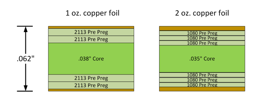
A typical 4-layer 1.6 mm PCB might have the following construction:
- Top layer: 1 oz copper (0.035 mm)
- Prepreg dielectric: 0.2 mm
- Inner layer 1: 1 oz copper
- Core dielectric: 1.1 mm
- Inner layer 2: 1 oz copper
- Prepreg dielectric: 0.2 mm
- Bottom layer: 1 oz copper
High-Frequency/RF PCBs:
These often use specialized dielectric materials with tight thickness tolerances to maintain consistent impedance characteristics. Thickness variations can significantly affect signal integrity in high-frequency applications.
Heavy Copper PCBs:
Boards with copper weights above 3 oz (0.105 mm) per layer may require adjustment to the overall thickness to accommodate the additional copper thickness, especially in multilayer configurations.
Flexible PCBs:
Flex circuits are typically much thinner than rigid boards, often in the range of 0.1 mm to 0.3 mm. The thickness is carefully controlled to maintain flexibility while providing adequate mechanical strength.
Rigid-Flex PCBs:
These hybrid boards combine rigid and flexible sections, requiring careful thickness management at transition areas. The rigid portions typically match standard thicknesses (like 1.6 mm), while the flexible sections are much thinner.
Metal-Core PCBs:
Used for high thermal dissipation applications, these boards incorporate a metal (usually aluminum) base layer. The overall thickness is dominated by the metal core, which may be several millimeters thick, with thin dielectric and copper layers on top.
High-Density Interconnect (HDI) PCBs:
HDI boards often use thinner dielectrics between layers to enable finer features and higher interconnection density. While individual layers are thinner, the overall board thickness may be similar to conventional boards due to the higher layer count.
Understanding these specialized considerations is crucial when designing or specifying PCBs for advanced applications where standard thickness guidelines may not apply.
Conclusion
PCB thickness, while seemingly a simple specification, plays a critical role in the performance, reliability, and manufacturability of electronic circuits. The common standard thickness of 1.6 mm has emerged as the industry workhorse due to its optimal balance of mechanical strength, component compatibility, and manufacturing efficiency. However, numerous applications require deviations from this standard, whether to meet space constraints, thermal requirements, or specialized mechanical needs.
Designers must consider the complete system requirements when selecting PCB thickness, including mechanical stresses, layer count, component leads, connector specifications, and thermal management needs. Understanding the standard thickness options, measurement techniques, and tolerances helps ensure that the manufactured boards will meet both electrical and mechanical requirements.
As electronic devices continue to evolve, pushing the boundaries of miniaturization, power density, and performance, PCB thickness will remain a key parameter in electronic design. The growing adoption of advanced technologies like HDI, rigid-flex, and embedded components will drive further innovation in PCB thickness optimization. By mastering the principles outlined in this article, engineers and designers can make informed decisions about PCB thickness that balance all relevant factors for their specific applications.
Ultimately, the “right” PCB thickness is the one that meets all technical requirements while being manufacturable at acceptable cost and lead time. Collaboration with experienced PCB manufacturers during the design phase can help identify the optimal thickness and avoid potential issues in production and assembly.