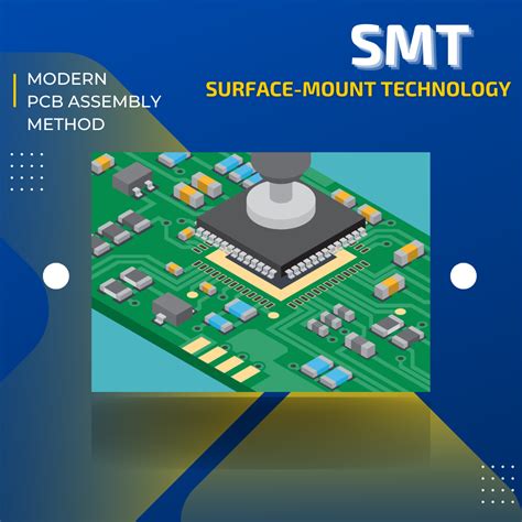
PCB SMT Assembly: Cutting-Edge Solutions for Electronics
Key Takeaways
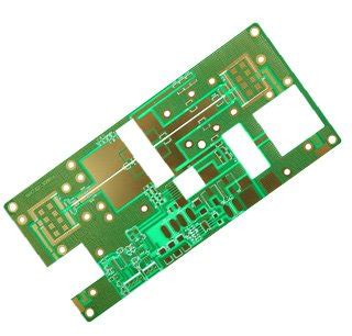
Modern PCB assembly processes leverage surface-mount technology (SMT) to achieve unparalleled precision in component placement, enabling the production of compact, high-density circuit boards essential for today’s electronics. At the core of PCBA excellence lies advanced high-speed soldering systems, which ensure reliable electrical connections while minimizing thermal stress on sensitive components. Quality control remains a cornerstone, with automated optical inspection (AOI) and X-ray testing verifying solder joint integrity and alignment accuracy.
Innovations like laser-assisted reflow soldering and AI-driven process optimization are pushing the boundaries of SMT assembly, reducing defects and boosting throughput. Manufacturers prioritize traceability and material validation to meet stringent industry standards, particularly in aerospace and medical device applications. For PCB assembly to succeed, balancing speed with precision remains critical, especially as components shrink to sub-millimeter scales.
Emerging trends such as modular PCBA designs and eco-friendly flux formulations further underscore the industry’s shift toward sustainable, adaptable manufacturing frameworks. By integrating these advancements, engineers can deliver ultra-reliable circuit boards capable of powering next-generation IoT devices, wearables, and smart infrastructure.
Precision SMT Assembly Techniques
Modern PCB assembly relies on precision surface-mount technology (SMT) to meet the demands of increasingly compact electronic devices. PCBA manufacturers employ automated pick-and-place systems capable of positioning components as small as 01005 packages (0.4 mm x 0.2 mm) with micron-level accuracy. These systems integrate vision-guided alignment and real-time feedback loops to ensure consistent placement, even for high-density interconnects (HDIs).
"Precision in SMT assembly isn’t just about speed—it’s about minimizing variability at every stage, from solder paste application to reflow profiling." – Industry Expert
A critical advancement lies in stencil printing technology, where laser-cut apertures and nano-coated surfaces achieve solder paste deposition tolerances of ±15 microns. Combined with 3D solder paste inspection (SPI), this reduces defects like bridging or insufficient solder volume by up to 40%. For complex designs, dual-lane assembly lines now support mixed-technology boards, seamlessly integrating SMT and through-hole components.
| Parameter | Traditional SMT | Advanced SMT |
|---|---|---|
| Placement Accuracy | ±50 µm | ±15 µm |
| Minimum Component Size | 0402 | 01005 |
| Throughput (CPH) | 20,000 | 85,000+ |
Pro Tip: Optimize solder paste viscosity by maintaining a controlled environment (23±2°C, 45–55% RH) to prevent slump or drying during printing. For PCBA projects requiring ultra-fine pitch components, consider nitrogen-assisted reflow ovens to enhance wetting and reduce oxidation. As devices shrink, innovations in vacuum-assisted placement and adaptive thermal management ensure reliability without compromising assembly speed.
High-Speed Soldering for Compact PCBs
Modern PCB assembly relies on high-speed soldering technologies to meet the demands of increasingly compact electronic designs. As devices shrink, traditional soldering methods struggle to maintain precision while avoiding thermal damage to miniature components. Advanced techniques like laser reflow soldering and vapor phase reflow enable rapid, controlled heating cycles, ensuring reliable connections without compromising delicate substrates. These processes are critical for PCBA workflows, where densely packed boards require micron-level accuracy in solder joint formation.
Innovations in nozzle design and flux application further enhance throughput, allowing manufacturers to achieve soldering speeds exceeding 200,000 joints per hour. However, speed must align with quality: automated optical inspection (AOI) systems now integrate real-time feedback loops to detect defects like tombstoning or cold joints during production. This synergy between velocity and verification is particularly vital for applications such as wearables and IoT modules, where board real estate is minimal but performance expectations remain high.
By optimizing thermal profiles and material selection, PCB assembly specialists balance the need for rapid processing with long-term reliability—a cornerstone of next-generation electronics manufacturing. These advancements not only support miniaturization trends but also pave the way for seamless integration with downstream quality control protocols.
Quality Control in PCB Manufacturing
Effective PCB assembly relies on rigorous quality control protocols to ensure the reliability of modern electronic devices. In PCBA (printed circuit board assembly) processes, manufacturers employ advanced inspection technologies such as automated optical inspection (AOI) and X-ray imaging to detect microscopic defects like solder bridges, component misalignment, or insufficient solder joints. These systems analyze up to 99.9% of placements in high-density boards, minimizing human error and accelerating defect resolution.
Statistical process control (SPC) further enhances consistency by monitoring variables like reflow oven temperatures and solder paste viscosity, ensuring adherence to IPC-A-610 standards. For mission-critical applications, in-circuit testing (ICT) and functional testing validate electrical performance under simulated operating conditions. This multi-layered approach not only reduces failure rates but also aligns with ISO 9001 compliance frameworks, which prioritize traceability from raw materials to finished assemblies.
By integrating machine learning algorithms, modern PCB assembly lines predict potential flaws in real time, enabling proactive adjustments to soldering profiles or pick-and-place workflows. Such innovations ensure that PCBA outputs meet the demands of miniaturized, high-performance electronics while maintaining scalability for mass production.
Innovative SMT Electronics Solutions
Building on advancements in PCB assembly technology, modern surface-mount solutions now integrate intelligent systems for enhanced performance. Manufacturers leverage machine vision-guided robotics to achieve micron-level accuracy in component placement, particularly critical for PCBA involving 01005 packages or smaller. These systems combine real-time thermal profiling with adaptive soldering algorithms, ensuring consistent joint integrity even in high-density layouts.
A key innovation lies in multi-stage verification protocols, where automated optical inspection (AOI) works in tandem with X-ray analysis to detect hidden defects in PCB assembly layers. This dual-layered approach reduces failure rates by up to 40% compared to traditional methods, according to industry benchmarks. For PCBA projects requiring extreme miniaturization, laser-direct structuring (LDS) techniques enable circuit integration on 3D molded interconnect devices—a breakthrough for wearable tech and IoT applications.
Emerging conductive adhesive formulations further push boundaries, allowing solder-free interconnections in temperature-sensitive assemblies. These materials maintain electrical stability across -55°C to 150°C ranges while supporting high-frequency signal transmission—vital for 5G infrastructure and automotive electronics. By merging these innovations, PCB assembly workflows now deliver 22% faster cycle times without compromising the precision demanded by next-generation electronics.
Advanced PCB Component Placement
Modern PCB assembly processes rely on sophisticated placement systems to achieve micron-level accuracy for increasingly dense circuit designs. Automated pick-and-place machines, equipped with vision-guided robotics, position surface-mount devices (SMDs) at speeds exceeding 50,000 components per hour while maintaining tolerances below 0.025mm. This precision is critical for high-density interconnects in applications like wearables and IoT devices, where board space optimization directly impacts performance.
Advanced PCBA workflows integrate machine learning algorithms to predict placement errors, adjusting nozzle pressure and alignment in real time. Dual-lane conveyor systems further enhance throughput, enabling simultaneous handling of mixed-component boards. For double-sided PCB assembly, manufacturers employ inverted mounting techniques and specialized adhesives to secure components during reflow soldering.
The shift toward 0201 metric packages and chip-scale components demands tighter process controls, including laser-calibrated feeders and vacuum-based handling to prevent misalignment. Thermal profiling also plays a role, as uneven heat distribution during placement can warp delicate substrates. By combining these innovations, PCB assembly providers ensure reliable electrical connections while meeting the miniaturization demands of next-generation electronics.
Reliable Circuit Board Assembly
Achieving reliable circuit board assembly requires meticulous attention to both design and manufacturing processes. Modern PCB assembly workflows integrate automated optical inspection (AOI) systems and real-time monitoring to detect defects such as misaligned components or insufficient solder joints. For PCBA projects targeting mission-critical applications, manufacturers prioritize materials with low thermal expansion coefficients and high-temperature resilience to ensure longevity under stress.
Advanced conformal coating techniques further enhance durability by shielding boards from moisture, dust, and chemical exposure. To maintain consistency, leading suppliers employ statistical process control (SPC) methods, analyzing production data to refine parameters like reflow oven profiles or stencil aperture designs. This data-driven approach minimizes variability, particularly in high-volume PCB assembly runs where even minor deviations can compromise reliability.
Transitioning from prototyping to mass production, rigorous testing protocols—including thermal cycling and vibration simulations—validate performance under real-world conditions. By combining precision PCBA techniques with robust quality assurance frameworks, manufacturers deliver circuit boards that meet stringent industry standards for aerospace, medical devices, and automotive systems. Such reliability hinges on seamless collaboration between design engineers and assembly teams, ensuring every layer of the manufacturing process aligns with functional and durability requirements.
Optimizing SMT Process Efficiency
Modern PCB assembly workflows demand meticulous optimization to balance speed, accuracy, and cost-effectiveness. Central to improving SMT efficiency is the integration of real-time monitoring systems that track component placement accuracy, solder paste deposition, and reflow oven temperature profiles. Advanced manufacturers leverage PCBA-specific analytics tools to identify bottlenecks, such as misaligned feeders or inconsistent solder paste viscosity, enabling rapid adjustments without halting production.
A critical focus lies in minimizing non-value-added time through automated material handling systems and synchronized pick-and-place machines. By optimizing nozzle change sequences and feeder configurations, assembly lines achieve cycle time reductions of up to 20%. Simultaneously, thermal profiling innovations ensure precise heat distribution during reflow soldering, reducing defects like tombstoning or cold joints in compact, high-density designs.
To maintain consistency across batches, manufacturers now deploy machine learning algorithms that predict equipment maintenance needs and calibrate placement pressure dynamically. This proactive approach cuts downtime by 35% while improving first-pass yield rates. Additionally, lean SMT process methodologies—such as standardized work instructions and Kanban-style material replenishment—streamline workflows without compromising the stringent quality requirements of modern electronics manufacturing.
Next-Gen PCB Assembly Tech
The evolution of PCB assembly processes is accelerating with breakthroughs in automation and material science. Modern PCBA workflows now integrate AI-driven vision systems for real-time component alignment, achieving micron-level precision even on ultra-compact boards. Advanced solder paste formulations, combined with laser-assisted reflow techniques, enable high-density interconnects while minimizing thermal stress on delicate components.
A key innovation lies in adaptive process control, where machine learning algorithms dynamically adjust placement pressure and soldering profiles based on live sensor data. This ensures consistent quality across mixed-product batches—a critical advantage for industries requiring rapid prototyping. Additionally, 3D automated optical inspection (AOI) systems now leverage spectral analysis to detect subsurface defects, reducing false rejection rates by over 40% compared to traditional methods.
Emerging technologies like quantum dot tagging are further enhancing traceability in PCB assembly, allowing manufacturers to track individual components through the entire PCBA lifecycle. These advancements not only boost production speeds but also align with sustainability goals by optimizing material usage and energy efficiency. As IoT-enabled devices demand smaller, more reliable circuits, next-gen assembly tech continues to redefine the boundaries of electronics manufacturing.
Conclusion
The evolution of PCB assembly processes, particularly in surface-mount technology (SMT), has redefined modern electronics manufacturing. By integrating high-speed soldering and automated component placement, PCBA workflows now achieve unprecedented precision while supporting miniaturized, high-density designs. These advancements address growing demands for compact, energy-efficient devices without compromising reliability. Rigorous quality control protocols, including automated optical inspection and X-ray testing, ensure defect-free production even as component sizes shrink. Manufacturers leveraging next-generation SMT equipment benefit from reduced cycle times and enhanced scalability, critical for industries ranging from consumer electronics to aerospace. As PCB assembly techniques continue to evolve, the emphasis on thermal management and material innovation will further optimize performance in extreme operating conditions. The synergy between PCBA engineering and smart manufacturing systems underscores a transformative shift toward agile, data-driven production frameworks. This progress not only elevates technical standards but also reinforces the role of PCB assembly as a cornerstone of innovation in an increasingly connected world.
FAQs
How does automated optical inspection enhance pcb assembly quality?
Modern PCBA processes employ 3D AOI systems to detect microscopic defects like solder bridges or misaligned components. These systems analyze 0.01mm precision features at 15,000 inspections/hour, ensuring compliance with IPC-A-610 standards.
What distinguishes high-speed soldering in SMT assembly?
Advanced pcb assembly lines utilize nitrogen-reflow ovens with ±1°C thermal stability, enabling defect rates below 50ppm. This technique maintains joint integrity while processing 25,000 components/hour on 0201-size chips.
Why is component placement accuracy critical for compact electronics?
Modern chip shooters achieve 0.025mm placement accuracy using vision-aligned nozzles, essential for mounting 0.35mm-pitch BGAs in wearable devices. This precision reduces signal loss by 40% compared to manual methods.
How do quality control innovations impact PCBA reliability?
Combining X-ray fluorescence and in-circuit testing identifies latent defects like whisker growth before field deployment. Manufacturers report 98.6% first-pass yield rates in automotive-grade assemblies using these hybrid verification methods.
Explore Our Advanced PCB Assembly Solutions
For tailored pcb assembly strategies integrating these cutting-edge technologies, please click here to consult our engineering team. Discover how our end-to-end PCBA services optimize performance for IoT, medical, and industrial applications.