Cutting-Edge PCB Assembly: Trusted Global Industry Leaders

Key Takeaways
The global PCB assembly landscape is defined by manufacturers that combine precision engineering with scalable production to meet evolving technological demands. Leading PCBA providers distinguish themselves through advanced SMT solutions, achieving micron-level accuracy for high-density interconnect (HDI) boards and miniaturized components. These firms prioritize ISO-certified processes and IPC-A-610 compliance, ensuring reliability across automotive, aerospace, and IoT applications.
Tip: When evaluating PCB assembly services, verify certifications for lead-free manufacturing and thermal management capabilities to future-proof your designs.
A critical advantage among top-tier companies lies in rapid prototyping ecosystems, which integrate automated optical inspection (AOI) and 3D solder paste testing to reduce time-to-market by up to 40%. Innovations like embedded component packaging and flexible hybrid electronics further position these leaders at the forefront of next-generation device development.
"The shift toward IoT-enabled PCB assemblies demands partnerships with suppliers offering end-to-end traceability and real-time production analytics."
As industries adopt 5G-ready PCBA designs and AI-driven quality control, selecting a trusted global partner with multi-region manufacturing hubs becomes essential to mitigate supply chain risks. This strategic alignment ensures seamless scalability from prototyping to full-scale production.

Global PCB Assembly Pioneers
The evolution of PCB assembly has been driven by a select group of global innovators who combine technical mastery with scalable manufacturing frameworks. These industry leaders excel in delivering PCBA solutions that meet rigorous quality benchmarks while addressing the demands of sectors like aerospace, automotive, and IoT. By integrating automated optical inspection (AOI) and surface-mount technology (SMT), they ensure precision across high-volume production runs and complex multilayer designs.
| Company | Key Strengths | Global Reach |
|---|---|---|
| Company A | High-Density Interconnect (HDI) | 15+ Countries |
| Company B | Flexible PCB Solutions | 20+ Facilities |
| Company C | Military-Grade Reliability | 12+ R&D Centers |
Geographic diversification remains critical, with pioneers operating advanced facilities across Asia, North America, and Europe to minimize supply chain disruptions. Their focus on smart manufacturing—leveraging AI-driven process optimization and real-time analytics—enables faster turnaround times without compromising PCB assembly accuracy. As industries increasingly prioritize miniaturization and energy efficiency, these innovators are redefining standards for PCBA workflows, seamlessly bridging prototyping and mass production. This strategic alignment positions them as indispensable partners for next-generation electronics development, setting the stage for deeper explorations of SMT advancements and rapid prototyping methodologies in subsequent sections.
Advanced SMT Solutions Experts
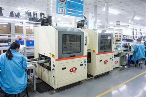
Leading PCB assembly providers distinguish themselves through mastery of Surface Mount Technology (SMT), a cornerstone of modern electronics manufacturing. By leveraging high-speed pick-and-place systems and precision solder reflow processes, these specialists deliver PCBA solutions optimized for compact, high-density designs. Innovations like automated optical inspection (AOI) and 3D X-ray verification ensure micron-level accuracy, critical for applications ranging from IoT devices to aerospace systems.
Top-tier manufacturers integrate advanced SMT workflows with intelligent process controls, enabling real-time adjustments for temperature profiles and component alignment. This technical prowess supports the assembly of ultra-fine-pitch components, including 01005 passives and micro-BGA packages, while maintaining yields above 99.95%. For industries requiring stringent reliability, PCB assembly experts employ thermal cycling tests and in-circuit testing (ICT) to validate performance under extreme conditions.
The shift toward Industry 4.0-ready SMT lines further enhances scalability, with IoT-enabled machines providing predictive maintenance analytics and traceability across global supply chains. As demand grows for miniaturized, high-frequency electronics, these PCBA leaders continue to refine hybrid approaches that combine SMT with through-hole and flexible circuit integration—ensuring seamless compatibility with next-generation 5G, AI, and automotive innovations.
Electronics Prototyping Leaders
In the fast-paced world of electronics development, PCB assembly innovators specializing in prototyping play a pivotal role in bridging conceptual designs with functional products. Leading companies in this space leverage rapid iteration cycles and PCBA expertise to deliver prototypes that meet stringent performance benchmarks while accelerating time-to-market. By integrating advanced testing protocols, such as automated optical inspection (AOI) and functional validation, these firms ensure prototypes align with end-use requirements, from aerospace-grade durability to consumer electronics miniaturization.
A hallmark of top-tier providers is their ability to balance speed with precision, offering 24–72-hour turnaround times without compromising on PCB assembly quality. This agility is critical for startups and enterprises alike, enabling iterative testing of complex designs featuring high-density interconnects (HDI) or mixed-technology boards. Furthermore, partnerships with PCBA specialists often include access to cutting-edge materials, such as flexible substrates or thermally conductive laminates, which are essential for next-generation IoT, wearables, and medical devices.
By prioritizing seamless collaboration between engineering teams and clients, prototyping leaders streamline the transition from prototype to mass production, ensuring scalability and compliance with global manufacturing standards. Their expertise in optimizing design-for-manufacturability (DFM) principles underscores their role as indispensable partners in the electronics innovation ecosystem.

Top PCB Manufacturing Innovations
The evolution of PCB assembly technologies continues to redefine electronics production, with industry leaders integrating breakthroughs in material science, automation, and miniaturization. Cutting-edge additive manufacturing techniques now enable the creation of ultra-thin, flexible substrates, while PCBA processes leverage embedded component technology to reduce footprint and enhance signal integrity. Innovations like high-density interconnect (HDI) designs and laser-direct imaging (LDI) systems are pushing the boundaries of multilayer board precision, achieving trace widths below 15µm.
A critical advancement lies in the adoption of IoT-enabled smart factories, where real-time analytics optimize PCB assembly workflows, minimizing defects and accelerating time-to-market. Leading manufacturers are also pioneering eco-conscious methods, such as halogen-free laminates and lead-free soldering, to meet stringent global sustainability standards. For PCBA applications in aerospace and medical devices, nanocoating technologies provide unmatched protection against environmental stressors, ensuring reliability in extreme conditions.
These innovations align with the growing demand for rapid prototyping and scalable production, enabling seamless transitions from low-volume PCB assembly to mass manufacturing. As next-gen technologies like 5G and AI drive component complexity, the industry’s shift toward automated optical inspection (AOI) and machine learning-driven QA systems underscores its commitment to precision and adaptability.
Precision PCB Assembly Standards
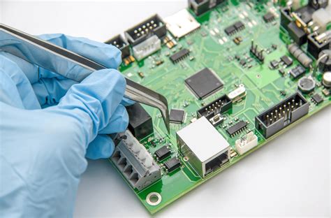
Modern PCB assembly processes demand adherence to rigorous quality benchmarks to ensure reliability in increasingly complex electronic systems. Industry leaders prioritize compliance with IPC-A-610 and ISO 9001 standards, which govern everything from solder joint integrity to component placement accuracy. Advanced PCBA workflows integrate automated optical inspection (AOI) and X-ray testing, enabling micron-level defect detection for high-density interconnect (HDI) boards.
Key to precision is the harmonization of surface-mount technology (SMT) with mixed-technology assemblies, balancing speed and accuracy across prototyping and mass production phases. Manufacturers leverage laser-direct imaging (LDI) and controlled impedance routing to maintain signal integrity in 5G and IoT applications. Material selection—such as high-Tg laminates and halogen-free substrates—further ensures thermal stability in harsh operating environments.
Transitioning toward smart factories, top-tier providers employ machine learning algorithms to optimize pick-and-place operations, reducing cycle times while achieving ±0.025mm placement tolerances. This synergy of cutting-edge machinery and standardized protocols positions PCB assembly as the backbone of next-generation electronics, where even minor deviations can impact end-product performance. As industries push for miniaturization, these precision frameworks become critical in sustaining innovation across aerospace, medical devices, and automotive sectors.
Next-Gen PCB Technologies Unveiled
The evolution of PCB assembly processes is accelerating as manufacturers integrate breakthrough innovations to meet the demands of advanced applications. Emerging technologies like additive manufacturing and laser-direct structuring are redefining PCBA workflows, enabling ultra-high-density interconnects (HDI) and miniaturized designs critical for IoT devices and 5G infrastructure. Leading providers now leverage embedded component packaging to embed passive components directly into substrates, reducing footprint while enhancing signal integrity.
Another transformative shift involves the adoption of AI-driven quality control systems, which analyze solder joint integrity and component placement accuracy in real time during PCB assembly. These systems minimize defects in complex multi-layer boards, particularly for aerospace and medical applications where reliability is non-negotiable. Additionally, advancements in flexible hybrid electronics (FHE) are merging rigid PCBA techniques with stretchable circuits, unlocking possibilities in wearable tech and foldable displays.
To stay competitive, top-tier PCB assembly firms are also prioritizing eco-conscious practices, such as halogen-free laminates and lead-free soldering, aligning with global sustainability mandates. As these next-gen solutions mature, they reinforce the industry’s capacity to deliver faster prototyping cycles and scalable production without compromising precision—key traits for innovators shaping tomorrow’s electronics landscape.
Trusted Global PCB Partners
In an interconnected electronics ecosystem, establishing partnerships with PCB assembly specialists who demonstrate proven cross-border capabilities has become critical for OEMs navigating complex global supply chains. Leading PCBA providers distinguish themselves through multi-regional compliance, maintaining ISO-certified facilities across Asia, Europe, and the Americas to ensure seamless production scalability and risk mitigation. These partners combine precision manufacturing rigor with localized logistics networks, enabling just-in-time delivery for industries ranging from automotive to aerospace.
The most trusted collaborators excel in adaptive problem-solving, addressing challenges like component shortages through strategic alliances with semiconductor distributors and alternative sourcing databases. Their expertise in PCB assembly extends beyond technical execution, incorporating real-time traceability systems that align with IPC-A-610 and IATF 16949 standards. By integrating AI-driven defect detection and blockchain-based quality documentation, these global partners reduce time-to-market while preserving the integrity of high-density interconnect (HDI) designs.
For innovators requiring PCBA solutions across multiple jurisdictions, selecting a partner with unified process controls ensures consistency in solder joint reliability, thermal management, and EMI shielding performance. Forward-looking providers further strengthen global trust through sustainability initiatives, implementing lead-free HASL finishes and recyclable substrate strategies that meet evolving EU RoHS and REACH directives. This transnational operational framework positions them as indispensable allies in scaling next-generation IoT and 5G deployments worldwide.
Rapid PCB Prototyping Solutions
In today’s fast-paced electronics landscape, PCB assembly innovators are redefining product development through agile prototyping methodologies. Leading PCBA providers combine automated optical inspection (AOI) systems with laser-direct imaging to reduce iteration cycles by up to 65%, enabling functional prototypes within 24–72 hours. These solutions integrate PCB assembly workflows with real-time design validation, allowing engineers to test form factors, thermal performance, and signal integrity early in the R&D phase. For high-density interconnect (HDI) designs, advanced manufacturers leverage 3D printing for rapid via formation and impedance-controlled layer stackups, ensuring compliance with mil-aerospace or medical-grade specifications.
The adoption of AI-powered DFM (design-for-manufacturing) checks further accelerates timelines by preemptively addressing potential solder mask misalignments or component placement conflicts. By merging PCBA expertise with modular prototyping platforms, global partners deliver scalable pre-production batches that maintain the precision of mass-manufactured boards. This synergy between speed and accuracy not only slashes time-to-market but also provides a critical bridge for startups and enterprises transitioning from concept validation to volume production.
Conclusion
As the electronics manufacturing landscape evolves, selecting partners with proven expertise in PCB assembly remains critical for achieving technological excellence. Industry leaders distinguish themselves through innovative PCBA processes that integrate cutting-edge automation, stringent quality controls, and adaptive supply chain strategies. These providers not only excel in precision manufacturing but also prioritize scalability, enabling seamless transitions from rapid prototyping to full-scale production. By leveraging advancements in SMT solutions and materials science, top-tier companies address the growing demands for miniaturization, thermal management, and high-frequency performance in next-generation devices. Their global footprint ensures compliance with regional regulatory standards while maintaining cost-efficiency for diverse markets. For businesses navigating the complexities of IoT, automotive electronics, or AI-driven hardware, collaboration with trusted PCB assembly specialists becomes a strategic imperative—ensuring both technical superiority and accelerated time-to-market in an increasingly competitive ecosystem.
FAQs
What factors determine a top-tier PCB assembly provider?
Leading companies prioritize precision manufacturing, adherence to IPC-A-610 standards, and certifications like ISO 9001. They also invest in advanced SMT equipment and offer end-to-end traceability for complex PCBA projects.
How does PCB assembly differ from PCBA?
PCB assembly refers to the process of populating a bare board, while PCBA (Printed Circuit Board Assembly) denotes the completed, functional unit. Top providers excel in both stages, ensuring seamless integration from design to final testing.
What are typical lead times for prototyping and mass production?
Rapid prototyping can take 3–7 days with expedited PCB assembly services, while high-volume PCBA production ranges from 2–6 weeks, depending on design complexity and component availability.
Which quality certifications should reliable PCB assembly partners hold?
Look for UL listing, ISO 13485 (for medical devices), and IATF 16949 (automotive). These ensure compliance with industry-specific PCBA reliability and safety requirements.
How do advanced technologies like HDI or flexible PCBs impact assembly?
High-Density Interconnect (HDI) and flexible circuits demand specialized PCB assembly techniques, including laser drilling and precision soldering. Leading manufacturers leverage these to support next-gen applications like wearables and IoT.
What cost factors should be evaluated when selecting a PCBA partner?
Beyond per-unit pricing, consider tooling fees, minimum order quantities, and testing protocols. Transparent providers offer scalable solutions for both prototyping and large-scale PCB assembly.
Explore Advanced PCB Assembly Solutions
Please click here to learn more about our industry-leading PCB assembly capabilities, including rapid prototyping and high-mix production.