Gold Finger PCB: A Comprehensive Guide to Design, Applications, and Manufacturing
Introduction to Gold Finger PCBs
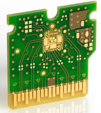
Gold Finger Printed Circuit Boards (PCBs) represent a specialized type of circuit board that features gold-plated contacts along one or more edges. These distinctive gold-plated connectors, resembling “fingers,” serve as the critical interface between the PCB and other electronic components or devices. The technology has become increasingly important in modern electronics due to its superior conductivity, durability, and resistance to corrosion compared to other contact methods.
The gold fingers on these PCBs are not merely aesthetic features; they perform essential electrical and mechanical functions in various electronic devices. From desktop computer components to sophisticated industrial equipment, gold finger PCBs enable reliable connections that can withstand repeated insertion and removal cycles. The gold plating, typically applied over a nickel base layer, provides excellent surface conductivity while protecting the underlying copper from oxidation and wear.
This article will explore the technical aspects, manufacturing processes, design considerations, and diverse applications of gold finger PCBs, providing a comprehensive understanding of this crucial electronic component.
Technical Specifications of Gold Finger PCBs
Gold Plating Thickness and Composition
The gold plating on PCB fingers typically ranges from 3 to 50 microinches (0.076 to 1.27 microns) in thickness. This plating usually consists of:
- Hard gold (cobalt-hardened): 99.7% gold with 0.3% cobalt, used for most applications requiring durability
- Soft gold (pure gold): 99.9% gold, used for wire bonding applications
- Electroless nickel immersion gold (ENIG): An alternative for some applications
The gold is always plated over a nickel barrier layer (150-200 microinches) that prevents copper diffusion and enhances durability.
Dimensional Standards
Gold finger PCBs adhere to strict dimensional standards:
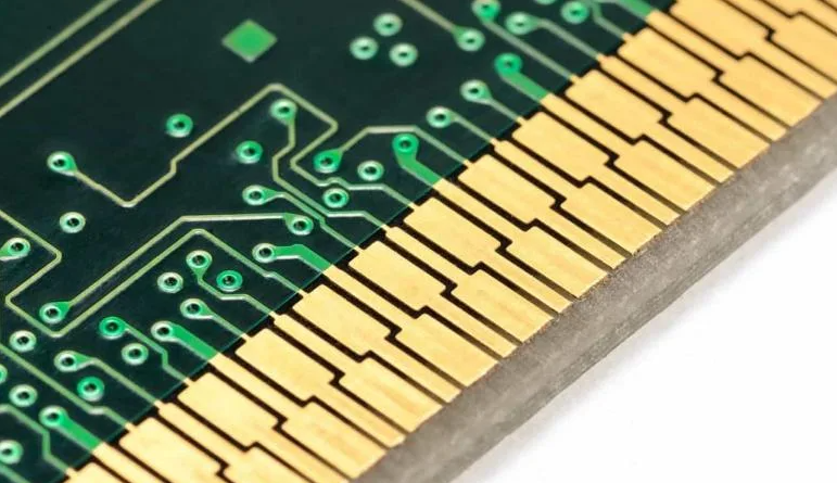
- Finger width: Typically 0.8mm to 1.5mm
- Finger spacing: Usually 0.8mm to 1.5mm between contacts
- Length: Varies by application but commonly 5-10mm
- Bevel angle: Standard 30° or 45° chamfer for easier insertion
Electrical Properties
- Contact resistance: <20mΩ for high-quality gold fingers
- Current carrying capacity: 1-3A per finger (depends on size and plating)
- Voltage rating: Typically up to 300V between adjacent fingers
Manufacturing Process of Gold Finger PCBs
Step 1: Substrate Preparation
The process begins with standard PCB fabrication:
- Laminate selection (typically FR-4)
- Copper cladding and patterning
- Drilling and through-hole plating
- Solder mask application
Step 2: Nickel Plating
Before gold deposition, a nickel layer is applied:
- Cleaning and surface preparation
- Electroless or electrolytic nickel plating (5-7μm thickness)
- Rinsing and quality inspection
Step 3: Gold Plating
The critical gold plating process involves:
- Activation of nickel surface
- Electrolytic gold plating (hard gold) or immersion gold (soft gold)
- Controlled thickness deposition
- Final rinsing and drying
Step 4: Beveling and Final Processing
- Precision edge beveling (30° or 45°)
- Electrical testing and continuity checks
- Visual inspection under magnification
- Packaging with protective coverings
Design Considerations for Gold Finger PCBs
Layout Guidelines
- Keep gold fingers at least 0.5mm away from other copper features
- Avoid placing vias or components near the contact area
- Design for appropriate strain relief to prevent cracking
- Consider insertion force requirements in mechanical design
Material Selection
- Base material: Typically FR-4, but high-frequency applications may require specialized laminates
- Nickel underplating: 5-7μm thickness for optimal performance
- Gold type selection based on application requirements
Reliability Factors
- Minimum 25μm gold thickness for high-cycle applications
- Proper surface finish selection adjacent to gold fingers
- Environmental considerations (humidity, temperature, contaminants)
Applications of Gold Finger PCBs
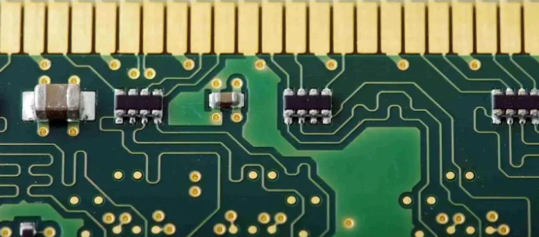
Computer Hardware
- Memory modules (DIMM, SIMM, RIMM)
- Graphics cards (PCIe interfaces)
- Expansion cards and daughterboards
- Solid-state drive connectors
Consumer Electronics
- Game cartridges and console connectors
- Smartphone and tablet docking stations
- Digital camera memory card interfaces
- High-end audio equipment connections
Industrial and Automotive
- Industrial control system backplanes
- Automotive ECU connectors
- Test and measurement equipment
- Aerospace avionics systems
Telecommunications
- Network interface cards
- Router and switch modules
- Base station components
- Fiber optic transceiver interfaces
Advantages of Gold Finger PCBs
Superior Electrical Performance
- Low and stable contact resistance
- Excellent signal integrity for high-speed applications
- Reduced insertion loss compared to other finishes
Enhanced Durability
- Withstands 1,000+ insertion cycles (with proper gold thickness)
- Resistant to wear and fretting corrosion
- Maintains performance in harsh environments
Reliability Benefits
- Oxidation-resistant surface
- Consistent performance over time
- Reduced maintenance requirements
- Compatibility with various mating connectors
Challenges and Limitations
Cost Considerations
- Gold is a precious metal with significant material cost
- Additional processing steps increase manufacturing expenses
- Not cost-effective for low-end consumer products
Technical Limitations
- Limited to edge connector applications
- Requires precise mechanical tolerances
- Not suitable for all environmental conditions (certain chemicals can affect performance)
Alternative Technologies
- ENIG (Electroless Nickel Immersion Gold) for some applications
- Selective gold plating to reduce costs
- Other surface finishes (OSP, HASL, immersion silver) for less demanding uses
Quality Control and Testing
Visual Inspection
- Microscope examination for plating uniformity
- Check for proper bevel angle and edge quality
- Verification of gold color and surface defects
Electrical Testing
- Continuity testing of all contacts
- Insulation resistance between adjacent fingers
- Contact resistance measurement
Mechanical Testing
- Insertion/extraction force measurement
- Wear testing for high-cycle applications
- Adhesion testing of gold plating
Environmental Testing
- Temperature cycling
- Humidity exposure
- Corrosion resistance tests
Future Trends in Gold Finger PCB Technology
Material Innovations
- Development of gold alloy platings for enhanced performance
- Alternative precious metal coatings
- Nanotechnology applications for thinner, more durable coatings
Manufacturing Advancements
- More precise plating control techniques
- Automated inspection systems
- Environmentally friendly processing methods
Application Expansion
- Higher density interconnects
- Miniaturization for portable devices
- Integration with flexible PCB technologies
Conclusion
Gold Finger PCBs remain an essential technology in modern electronics, offering unmatched reliability and performance for critical interconnect applications. While the technology carries higher costs than some alternatives, its benefits in demanding applications justify the investment. As electronic devices continue to evolve, gold finger technology adapts through material science advancements and manufacturing innovations.
Understanding the design principles, manufacturing processes, and application considerations for gold finger PCBs enables engineers to make informed decisions about their use in electronic products. Proper implementation of gold finger technology can significantly enhance product reliability and longevity in numerous industries.
The future of gold finger PCBs appears secure, with ongoing research focused on improving performance while reducing costs. As long as electronic devices require reliable, high-performance interconnects, gold finger technology will continue to play a vital role in electronic design and manufacturing.