Double-Sided Reflow Soldering in PCB Assembly: Techniques and Best Practices
Introduction to Double-Sided Reflow Technology
In the ever-evolving world of electronics manufacturing, double-sided reflow soldering has emerged as a critical process for producing compact, high-density printed circuit boards (PCBs). This advanced soldering technique allows components to be placed and soldered on both sides of a PCB, significantly increasing component density while reducing the overall size of electronic assemblies.
Double-sided reflow soldering represents a substantial improvement over traditional single-sided assembly methods, offering manufacturers the ability to create more complex and space-efficient electronic products. As consumer electronics continue to shrink in size while expanding in functionality, the demand for double-sided PCB assembly has grown exponentially across industries ranging from smartphones and wearables to automotive electronics and medical devices.
This article explores the complete double-sided reflow process, examining the technical challenges, innovative solutions, and best practices that ensure successful implementation. We’ll investigate the entire production workflow from design considerations through final inspection, providing a comprehensive guide for engineers and manufacturers looking to optimize their double-sided reflow operations.
Fundamentals of Double-Sided Reflow Process
Process Overview
Double-sided reflow soldering is a multi-stage manufacturing process that involves:
- Applying solder paste to one side of the PCB
- Placing surface mount components
- Reflow soldering the first side
- Flipping the board
- Repeating the process for the second side
- Performing a second reflow cycle
This approach differs fundamentally from single-sided reflow by requiring precise control of thermal profiles and component placement to prevent issues during the second soldering pass.
Key Advantages
The primary benefits driving adoption of double-sided reflow include:
- Space savings: Components on both sides can reduce PCB area by 30-50%
- Improved signal integrity: Shorter trace lengths for high-speed signals
- Enhanced thermal management: Heat-generating components can be distributed
- Cost reduction: Smaller PCB sizes lower material costs
- Design flexibility: Enables more complex circuit architectures
Technical Challenges
Despite its advantages, double-sided assembly presents unique challenges:
- Component retention: Preventing already-soldered parts from falling off during second reflow
- Thermal stress: Managing heat exposure for components undergoing two reflow cycles
- Shadowing effects: Larger first-side components affecting second-side soldering
- Process complexity: Additional steps increase potential failure points
Detailed Process Breakdown
Step 1: First Side Assembly
The initial stage mirrors traditional single-sided reflow:
- Solder Paste Application: Precise stencil printing deposits solder paste on first-side pads
- Component Placement: Pick-and-place machines position SMDs with high accuracy
- Pre-Reflow Inspection: Automated optical inspection (AOI) verifies paste and placement
- First Reflow: Carefully controlled thermal profile melts solder, forming joints
Critical considerations for first-side assembly include:
- Selecting components that can withstand two reflow cycles
- Planning for second-side thermal exposure
- Ensuring adequate adhesive for heavy/bulky components
Step 2: Board Flipping and Second Side Preparation
After first-side completion, boards undergo:
- Cooling: Controlled descent to room temperature stabilizes first-side joints
- Flipping: Precision handling prevents mechanical stress on soldered components
- Cleaning: Removal of any contaminants or oxides from second-side pads
- Paste Application: Second stencil printing (often with different stencil design)
Flipping mechanisms vary from simple manual rotation to sophisticated automated systems with vision-guided alignment. The choice depends on production volume and precision requirements.
Step 3: Second Side Assembly
The second-side process includes:
- Component Placement: Potentially different requirements than first side
- Adhesive Application: For vulnerable first-side components (if needed)
- Second Reflow: Modified thermal profile accounting for existing components
Second reflow presents the greatest technical challenge as it must:
- Form reliable second-side solder joints
- Avoid remelting first-side joints excessively
- Prevent thermal damage to sensitive components
- Manage differing thermal masses across the board
Thermal Profile Development
Dual-Side Profile Considerations
Developing appropriate thermal profiles requires addressing:
- Differential Heating: Accounting for variations in component thermal mass
- Peak Temperature Control: Ensuring sufficient heat for new joints without damaging existing ones
- Time Above Liquidus (TAL): Balancing joint formation with component safety
- Ramp Rates: Controlling thermal stress during heating and cooling
Profile Optimization Strategies
Effective approaches include:
- Zoned heating: Adjusting conveyor speed and zone temperatures
- Bottom-side heating: Reducing top-side thermal load
- Two-stage profiles: Customizing preheat and reflow segments
- Component-specific limits: Protecting sensitive devices
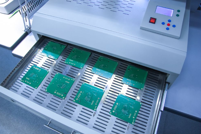
Advanced reflow ovens with multiple heating zones (typically 6-10) and independent top/bottom heating elements provide the control needed for double-sided processing.
Component Selection and Placement Strategies
Component Classification
For double-sided assembly, components are categorized by:
- Thermal Tolerance: Ability to withstand multiple reflow cycles
- Mass/Size: Impact on second-side soldering and retention
- Criticality: Importance to circuit function
- Orientation: Potential shadowing effects
Placement Guidelines
Best practices include:
- First-side placement: Larger, more thermally robust components
- Second-side placement: Smaller, temperature-sensitive devices
- Balanced distribution: Avoiding localized thermal mass concentrations
- Orientation: Minimizing shadowing of second-side pads
- Clearance: Ensuring adequate space for second-side reflow
Special Considerations
- Bottom-side BGA packages: Require careful thermal management
- Tall components: May interfere with second-side placement
- Mixed-technology boards: Incorporating through-hole components adds complexity

Solder Paste and Stencil Design
Paste Selection Criteria
Key factors for double-sided applications:
- Alloy composition: Typically SAC305 (Sn96.5/Ag3.0/Cu0.5) or similar
- Particle size: Type 3 or 4 for fine-pitch components
- Flux activity: Balanced to ensure cleaning while preventing oxidation
- Tack life: Sufficient for two-sided processing
Stencil Design Innovations
Advanced stencil features improve double-sided results:
- Step stencils: Varying thickness for different component types
- Nano-coated stencils: Enhancing paste release
- Aperture designs: Optimized for high-yield printing
- Under-bump deposition: For bottom-side BGA packages
Adhesive Solutions for Component Retention
Adhesive Types
Common options include:
- Thermally cured epoxies: Activated during reflow
- UV-curable adhesives: For selective curing
- Snap-cure materials: Fast processing
Application Methods
Precision dispensing techniques:
- Pin transfer: For high-volume production
- Screen printing: Patterned application
- Jet dispensing: Programmable, non-contact
- Syringe dispensing: For prototyping or low volume
Inspection and Quality Control
Process Verification Methods
Comprehensive inspection protocols include:
- Pre-reflow AOI: Verifying paste deposition and component placement
- Post-reflow AOI: Checking joint formation and component alignment
- X-ray inspection: For hidden joints (BGAs, QFNs)
- Automated optical inspection (AOI): For surface defects
- Functional testing: Validating electrical performance
Common Defects and Solutions
Frequent double-sided reflow issues:
- Tombstoning: Caused by uneven heating – addressed by thermal profile optimization
- Solder bridging: From excessive paste – corrected via stencil design
- Cold joints: Insufficient heat – resolved with profile adjustment
- Component shifting: During second reflow – prevented with adhesives
- Voiding: Particularly in BGA joints – minimized by paste selection and profile
Advanced Techniques and Innovations
Low-Temperature Soldering
Emerging approaches using:
- BiSn alloys: Melting point around 138°C
- SnIn alloys: For temperature-sensitive assemblies
- Transient liquid phase sintering: Creating high-melt joints from low-melt materials
Protective Atmospheres
Reflow environment enhancements:
- Nitrogen purging: Reducing oxidation
- Forming gas mixtures: Improving wetting
- Vacuum reflow: Minimizing voiding
Conductive Adhesives
Alternative joining methods:
- Isotropic conductive adhesives (ICAs)
- Anisotropic conductive films (ACFs)
- Nanoparticle inks
Industry Applications
Double-sided reflow enables advanced products across sectors:
- Consumer Electronics: Smartphones, tablets, wearables
- Automotive: Engine control units, ADAS systems
- Medical: Implantable devices, diagnostic equipment
- Aerospace: Avionics, satellite systems
- IoT Devices: Sensors, edge computing nodes
Future Trends
Emerging developments in double-sided assembly:
- 3D PCB structures: With multiple component layers
- Embedded components: Within the PCB substrate
- Advanced materials: For higher temperature tolerance
- AI-driven process optimization: Real-time profile adjustment
- Sustainable soldering: Lead-free and eco-friendly materials
Conclusion
Double-sided reflow soldering represents a sophisticated manufacturing solution that addresses the electronics industry’s relentless demands for miniaturization and increased functionality. By enabling component placement on both PCB surfaces, this technology provides substantial space savings and design flexibility while introducing unique process challenges.
Successful implementation requires careful consideration of thermal management, component selection, paste application, and inspection methodologies. As the technology continues to evolve with new materials, advanced equipment, and smarter process controls, double-sided reflow will remain essential for producing next-generation electronic devices.
Manufacturers adopting double-sided reflow must invest in proper equipment, staff training, and process development to overcome the technical hurdles. Those who master this complex but rewarding technology will gain significant competitive advantages in producing compact, high-performance electronic assemblies for an increasingly connected world.