Populated PCB: Design, Manufacturing, and Applications
Introduction to Populated PCBs
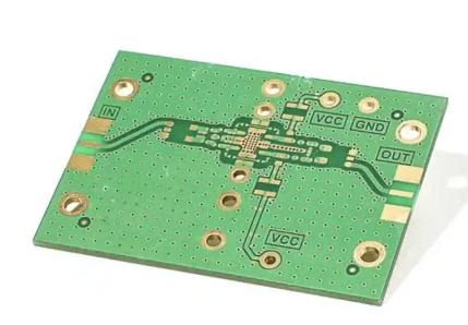
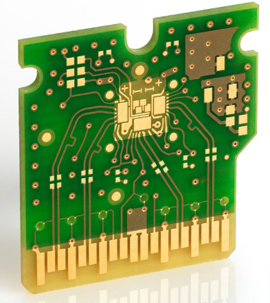
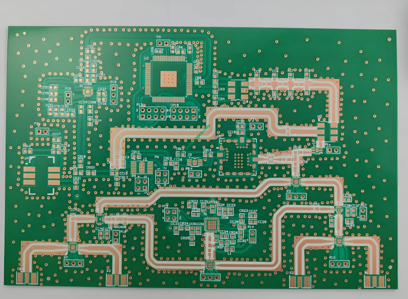
A Populated Printed Circuit Board (PCB) refers to a PCB that has all its electronic components assembled and soldered onto it, making it a fully functional circuit board. Unlike bare PCBs, which are just the board without any components, populated PCBs are ready for integration into electronic devices.
Populated PCBs are the backbone of modern electronics, found in everything from smartphones and computers to medical devices and automotive systems. This article explores the design considerations, manufacturing processes, testing methods, and applications of populated PCBs.
1. Design Considerations for Populated PCBs
Designing a populated PCB involves several critical steps to ensure functionality, reliability, and manufacturability.
1.1 Schematic Design
- The first step is creating a schematic diagram, which represents the electrical connections between components.
- Engineers use Electronic Design Automation (EDA) tools like Altium Designer, KiCad, or Eagle to design the circuit.
1.2 Component Selection
- Choosing the right components (resistors, capacitors, ICs, connectors) is crucial.
- Factors include power ratings, tolerances, package sizes, and availability.
1.3 PCB Layout and Routing
- The PCB layout defines the physical placement of components and traces.
- Key considerations:
- Signal integrity (minimizing noise and crosstalk).
- Power distribution (ensuring stable voltage levels).
- Thermal management (preventing overheating with proper heat sinks or vias).
1.4 Design for Manufacturing (DFM)
- DFM ensures the PCB can be efficiently manufactured.
- Rules include:
- Minimum trace widths and spacing (to avoid short circuits).
- Proper pad sizes (for reliable soldering).
- Component orientation (for automated assembly).
2. Manufacturing Process of Populated PCBs
The manufacturing of populated PCBs involves multiple stages, from PCB fabrication to component assembly.
2.1 PCB Fabrication
- Substrate Preparation – A fiberglass (FR4) or flexible substrate is cut to size.
- Copper Lamination – Copper layers are bonded to the substrate.
- Etching – Unwanted copper is removed to form conductive traces.
- Drilling – Holes for through-hole components and vias are drilled.
- Solder Mask Application – A protective layer is applied to prevent short circuits.
- Silkscreen Printing – Labels and component identifiers are printed.
2.2 Component Assembly
There are two primary methods for assembling components onto a PCB:
2.2.1 Surface Mount Technology (SMT)
- Components are placed directly onto the PCB surface.
- Process Steps:
- Solder Paste Application – A stencil deposits solder paste on pads.
- Pick-and-Place – A machine positions SMT components.
- Reflow Soldering – The board is heated to melt solder and form connections.
2.2.2 Through-Hole Technology (THT)
- Components with leads are inserted into drilled holes.
- Process Steps:
- Component Insertion – Done manually or via automated insertion machines.
- Wave Soldering – The PCB passes over a molten solder wave to create joints.
2.2.3 Mixed Assembly (SMT + THT)
- Many PCBs use both SMT and THT for different components.
2.3 Inspection and Testing
- Automated Optical Inspection (AOI) – Checks for soldering defects.
- X-ray Inspection – Used for hidden joints (e.g., BGA components).
- Functional Testing – Verifies the PCB operates as intended.
3. Testing and Quality Control
Ensuring the reliability of populated PCBs requires rigorous testing:
3.1 In-Circuit Testing (ICT)
- Tests individual components for correct values and connections.
3.2 Flying Probe Testing
- A non-contact method for checking electrical performance.
3.3 Burn-In Testing
- The PCB is operated under high stress to identify early failures.
3.4 Environmental Testing
- Tests resistance to temperature, humidity, and vibration.
4. Applications of Populated PCBs
Populated PCBs are used in nearly every electronic device, including:
4.1 Consumer Electronics
- Smartphones, laptops, TVs, and gaming consoles.
4.2 Automotive Industry
- Engine control units (ECUs), infotainment systems, and ADAS.
4.3 Medical Devices
- Pacemakers, MRI machines, and diagnostic equipment.
4.4 Industrial Automation
- Robotics, PLCs, and sensor systems.
4.5 Aerospace and Defense
- Avionics, satellite systems, and military communication devices.
5. Challenges in Populated PCB Manufacturing
Despite advancements, several challenges persist:
5.1 Miniaturization
- As devices shrink, PCB designs must accommodate smaller components (e.g., 01005 resistors).
5.2 High-Speed Design
- Managing signal integrity in high-frequency circuits (e.g., 5G, IoT).
5.3 Thermal Management
- Preventing overheating in densely packed PCBs.
5.4 Supply Chain Issues
- Component shortages can delay production.
6. Future Trends in Populated PCBs
Emerging technologies are shaping the future of PCB manufacturing:
6.1 High-Density Interconnect (HDI) PCBs
- More layers and finer traces for compact designs.
6.2 Flexible and Rigid-Flex PCBs
- Used in wearables and foldable electronics.
6.3 3D Printed Electronics
- Additive manufacturing for rapid prototyping.
6.4 AI and Machine Learning in PCB Design
- Automated optimization of layouts and fault detection.
Conclusion
Populated PCBs are essential in modern electronics, enabling the functionality of countless devices. From design and manufacturing to testing and applications, each step requires precision and expertise. As technology evolves, PCBs will continue to advance, supporting innovations in AI, IoT, and beyond. Understanding the intricacies of populated PCBs is crucial for engineers, manufacturers, and electronics enthusiasts alike.