PCB SMT Innovations Ensuring Reliable Electronics Production
Key Takeaways
Modern PCB assembly processes leverage SMT (Surface Mount Technology) innovations to address evolving demands for precision and reliability in electronics manufacturing. Central to this progress is the integration of automated optical inspection (AOI) systems, which minimize human error by detecting micro-scale defects in PCBA components. Advanced soldering techniques, such as laser reflow and vapor phase soldering, ensure consistent joint quality, directly enhancing product durability.
"Adopting intelligent SMT workflows isn’t optional—it’s a competitive necessity for manufacturers aiming to meet ISO-certified quality benchmarks."
Below is a comparison of traditional vs. modern SMT practices:
| Aspect | Traditional Approach | Innovative SMT Solution |
|---|---|---|
| Component Placement | Manual alignment | High-speed pick-and-place robots |
| Soldering Accuracy | Wave soldering | Precision laser-guided reflow |
| Quality Assurance | Sample-based testing | Real-time AOI with AI analytics |
For optimal results, manufacturers should prioritize PCBA partners offering closed-loop feedback systems, which synchronize design data with production metrics to preemptively resolve inconsistencies. Additionally, embedding IoT-enabled sensors in SMT lines enables predictive maintenance, reducing downtime by up to 30%. These advancements collectively ensure that modern electronics achieve tighter tolerances and longer operational lifespans, meeting both industrial and consumer reliability expectations.
PCB SMT Automated Assembly Advances
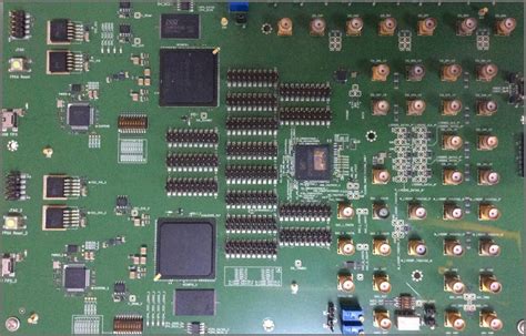
Modern PCB assembly processes have undergone transformative shifts with the integration of robotic pick-and-place systems and AI-driven optical inspection tools. These innovations enable PCBA manufacturers to achieve micron-level accuracy in component placement, significantly reducing human error while boosting throughput. Advanced conveyor systems now synchronize with real-time data analytics, optimizing material flow and minimizing downtime during high-volume production.
A critical advancement lies in the adoption of closed-loop feedback mechanisms, where sensors continuously monitor parameters like temperature and alignment, instantly adjusting machinery to maintain precision. This ensures consistent solder paste deposition and component orientation, vital for complex designs such as high-density interconnect (HDI) boards. Additionally, modular PCB assembly lines allow rapid reconfiguration for diverse product batches, enhancing flexibility without compromising speed.
The shift toward lights-out manufacturing exemplifies how PCBA facilities leverage fully automated workflows to operate 24/7 with minimal supervision. By integrating machine learning algorithms, these systems predict maintenance needs and preemptively address potential defects, elevating both yield rates and long-term product reliability. Such advancements not only streamline production but also lay the groundwork for scalable, error-resistant electronics manufacturing ecosystems.
Advanced Soldering Techniques for Durable PCBs
Modern PCB assembly relies on sophisticated soldering methods to ensure long-term reliability in electronic devices. Reflow soldering, for instance, has evolved to incorporate precise temperature profiling, minimizing thermal stress on sensitive components while achieving consistent joint formation. This technique is particularly critical in PCBA workflows, where high-density interconnects demand micron-level accuracy. Innovations like vapor phase soldering further enhance durability by using inert fluids to distribute heat uniformly, reducing oxidation risks in lead-free solder alloys.
Automated optical inspection (AOI) systems now integrate with soldering processes to detect microscopic defects, such as cold joints or bridging, which could compromise product lifespan. Additionally, the adoption of nanoparticle solder pastes improves wetting properties, ensuring stronger bonds between surface-mount devices (SMDs) and substrates. These advancements align with industry demands for PCB assembly solutions that withstand harsh environments, from automotive electronics to industrial IoT systems.
By optimizing solder alloy compositions and refining process parameters, manufacturers achieve higher first-pass yields in PCBA lines. This focus on precision not only elevates product durability but also reduces post-production rework, aligning with the broader shift toward zero-defect manufacturing in SMT workflows.
Precision-Driven SMT Manufacturing Solutions
Modern PCB assembly relies on precision-driven SMT manufacturing to meet the escalating demands for miniaturization and performance in electronics. Central to this approach are automated pick-and-place systems equipped with vision-guided robotics, ensuring micron-level accuracy when mounting components onto PCBA substrates. These systems integrate real-time feedback mechanisms to adjust for thermal expansion or material inconsistencies, minimizing placement errors even in high-speed production environments.
Advanced solder paste application techniques, such as laser-etched stencils and jet dispensing, further enhance process control by delivering precise volumes of solder alloy. This precision is critical for components like micro-BGAs or ultra-fine-pitch QFNs, where even minor deviations can compromise electrical connectivity. Pairing these methods with closed-loop reflow ovens ensures optimal thermal profiles, reducing voids and improving joint reliability across PCB assembly stages.
To maintain consistency, manufacturers now deploy inline inspection systems that leverage machine learning algorithms to detect defects at sub-20μm resolution. These tools correlate data from PCBA test points with production parameters, enabling predictive adjustments that preemptively address potential failures. Such integration of precision engineering and adaptive process control not only elevates yield rates but also aligns with the broader shift toward smart SMT workflows, seamlessly bridging to next-generation quality assurance protocols.
Next-Gen Quality Control in PCB SMT
Modern PCB assembly processes demand unprecedented precision, driving innovations in quality control systems tailored for SMT (Surface Mount Technology). Advanced inspection tools, such as automated optical inspection (AOI) and 3D X-ray imaging, now integrate machine learning algorithms to detect micron-level defects in PCBA (Printed Circuit Board Assembly). These systems analyze solder joint integrity, component misalignment, and trace connectivity in real time, reducing human error and accelerating throughput. By leveraging statistical process control (SPC), manufacturers gain actionable insights into production trends, enabling proactive adjustments to SMT parameters like reflow profiles or stencil designs.
The shift toward closed-loop feedback systems ensures defects flagged during inspection automatically trigger corrective actions in upstream PCB assembly stages. For instance, thermal profiling data from post-reflow inspections can dynamically optimize oven temperatures, enhancing solder joint reliability. Additionally, AI-powered anomaly detection identifies rare failure patterns that traditional methods might overlook, ensuring PCBA durability even in high-stress environments. Such innovations not only elevate product consistency but also align with Industry 4.0 standards, where data-driven quality control becomes a cornerstone of sustainable electronics manufacturing. Seamlessly bridging precision and scalability, these next-gen systems redefine reliability benchmarks across the SMT value chain.
Smart SMT Processes Enhancing Electronics Reliability
Modern PCB assembly workflows leverage intelligent SMT (Surface Mount Technology) processes to address critical challenges in electronics reliability. By integrating IoT-enabled sensors and AI-driven analytics, manufacturers now monitor PCBA (Printed Circuit Board Assembly) production lines in real time, detecting anomalies like component misalignment or solder defects before they escalate. Automated optical inspection (AOI) systems, paired with machine learning algorithms, achieve sub-micron accuracy in identifying microfractures or incomplete solder joints—issues traditionally undetectable in manual inspections.
These smart systems also optimize thermal profiling during reflow soldering, ensuring consistent heat distribution across complex PCB layouts. Adaptive process controls dynamically adjust parameters such as conveyor speed or paste viscosity, minimizing thermal stress on sensitive components. Additionally, predictive maintenance tools analyze equipment performance data to preemptively address wear in pick-and-place machines or stencil printers, reducing unplanned downtime.
By harmonizing precision SMT techniques with data-centric workflows, manufacturers achieve near-zero defect rates while extending the operational lifespan of electronic devices. This synergy between advanced automation and real-time quality assurance reinforces the durability of PCBA outputs, meeting stringent demands for aerospace, automotive, and medical applications.
SMT Innovations for High-Accuracy Production
Modern PCB assembly processes rely on precision-driven SMT innovations to meet escalating demands for miniaturization and performance. Central to these developments is the integration of AI-powered vision systems, which enable real-time component alignment with micron-level accuracy. These systems reduce placement errors in PCBA workflows by analyzing solder paste deposition and component orientation, ensuring consistent quality even with ultra-fine-pitch components. Advanced pick-and-place machines now leverage predictive algorithms to optimize nozzle selection and placement speed, minimizing mechanical drift over prolonged production cycles.
Another breakthrough lies in adaptive soldering technologies, where closed-loop thermal profiling maintains optimal reflow conditions for diverse board geometries. This eliminates cold joints and voiding, critical for high-reliability applications like automotive or aerospace electronics. Additionally, laser-assisted soldering systems are gaining traction for PCB assembly tasks requiring localized heat control, particularly in mixed-technology boards combining SMDs and through-hole components.
To sustain accuracy at scale, manufacturers are adopting digital twin simulations that mirror physical PCBA lines. These virtual models predict bottlenecks and calibrate machine parameters before deployment, slashing trial-and-error downtime. Coupled with IoT-enabled predictive maintenance, such innovations ensure that SMT equipment operates at peak precision, directly enhancing yield rates and long-term product durability. By harmonizing these advancements, the industry is redefining what’s achievable in high-accuracy electronics manufacturing.
Automated SMT Systems Elevating Product Durability
Modern PCB assembly processes increasingly rely on automated surface-mount technology (SMT) systems to ensure long-term reliability in electronic products. By integrating robotic placement systems and AI-driven calibration, manufacturers achieve micron-level precision in component positioning, minimizing mechanical stress and solder joint defects. These systems optimize PCBA durability by executing consistent solder paste application and reflow profiles, even for complex, high-density designs. Advanced thermal management algorithms further prevent overheating during assembly, preserving the integrity of sensitive components.
A key innovation lies in the synchronization of automated optical inspection (AOI) with real-time feedback loops. This combination identifies potential flaws—such as tombstoning or insufficient solder—before they escalate into field failures. For instance, adaptive systems adjust placement pressure dynamically based on component thickness variations, reducing board warpage risks. Such precision not only enhances product lifespan but also streamlines PCB assembly workflows, cutting downtime by 20–35% in high-volume production.
Moreover, smart SMT lines now incorporate predictive maintenance protocols, analyzing equipment performance data to preemptively address wear-related inaccuracies. By merging PCBA durability goals with Industry 4.0 principles, manufacturers deliver electronics capable of enduring harsh operational environments, from automotive vibration to industrial temperature cycling. This seamless integration of automation and quality assurance ensures each assembly phase contributes directly to end-product resilience.
Cutting-Edge SMT Technologies for Reliable Electronics
Modern PCB assembly processes leverage breakthroughs in surface-mount technology (SMT) to address escalating demands for precision and durability in electronics manufacturing. Innovations such as 3D solder paste inspection (SPI) systems now enable micron-level accuracy in depositing solder paste, minimizing defects like bridging or insufficient joints. Coupled with AI-driven automated optical inspection (AOI), these tools ensure consistent quality across high-volume PCBA production lines.
Advancements in thermocompression bonding and laser-assisted reflow soldering further enhance joint reliability, particularly for miniaturized components in IoT and automotive applications. Additionally, the integration of IoT-enabled process monitoring allows real-time adjustments to temperature profiles and placement accuracy, reducing thermal stress on sensitive components. These technologies work synergistically within automated SMT systems to achieve near-zero defect rates, a critical factor for industries requiring mission-critical electronics.
Furthermore, the adoption of adaptive stencil printing and multi-stage flux management ensures optimal material distribution during PCB assembly, preventing common failure points like cold solder joints. By combining these innovations, manufacturers achieve tighter tolerances in PCBA workflows, directly contributing to the longevity and performance of end products in harsh operating environments.
Conclusion
The evolution of PCB assembly technologies, particularly in SMT processes, underscores the industry’s commitment to precision and reliability in electronics manufacturing. As demonstrated throughout this discussion, innovations such as automated optical inspection (AOI) and predictive maintenance algorithms have redefined quality assurance in PCBA production. These advancements not only minimize human error but also optimize throughput, ensuring consistent performance across high-density circuit designs.
By integrating AI-driven process controls and real-time monitoring systems, manufacturers can preemptively address potential defects, reinforcing the durability of end products. Furthermore, the adoption of lead-free soldering techniques and thermally stable materials has elevated the resilience of SMT-based electronics, even in demanding environments. As the demand for compact, high-performance devices grows, the synergy between PCB assembly automation and data-centric quality frameworks will remain pivotal.
Looking ahead, the continuous refinement of PCBA workflows—from component placement accuracy to post-reflow validation—promises to bridge the gap between scalability and precision. This progression ensures that SMT innovations will keep pace with emerging technological requirements, solidifying their role as the backbone of reliable electronics production.
Frequently Asked Questions
How does automated PCB assembly improve manufacturing consistency?
Automated pick-and-place systems and reflow soldering technologies minimize human error, ensuring component placement accuracy within ±25μm. This precision directly enhances PCBA reliability by maintaining consistent solder joint quality across high-volume production runs.
What role do advanced soldering techniques play in PCB durability?
Innovations like laser soldering and vapor phase reflow create uniform thermal profiles, reducing thermal stress on components. These methods improve connection integrity in PCB assembly, particularly for high-density designs with 0201 metric components or micro-BGA packages.
How are quality control systems evolving in modern PCBA processes?
3D AOI (Automated Optical Inspection) systems now achieve 99.98% defect detection rates using machine learning algorithms. Combined with X-ray tomography for hidden joint analysis, these systems verify compliance with IPC-A-610 standards across all production stages.
Can smart PCB assembly systems adapt to different product requirements?
Modern cyber-physical production systems utilize real-time process monitoring to automatically adjust parameters like solder paste volume and placement pressure. This flexibility supports rapid changeovers between PCBA configurations while maintaining <50ppm defect rates.
Explore Advanced PCB Assembly Solutions
For tailored PCB assembly strategies integrating these innovations, please click here to consult our engineering team about optimizing your PCBA manufacturing workflow.