PCB Fabrication and Assembly: A Comprehensive Guide
Introduction to PCB Manufacturing
Printed Circuit Board (PCB) fabrication and assembly represent the cornerstone of modern electronics manufacturing. These intricate processes transform conceptual designs into functional electronic devices that power everything from smartphones to industrial machinery. PCB fabrication involves the creation of the bare board, while assembly refers to the process of populating that board with electronic components.
The global PCB market continues to expand rapidly, valued at approximately $72 billion in 2022 and projected to grow at a compound annual growth rate (CAGR) of 4.3% through 2030. This growth is driven by increasing demand across consumer electronics, automotive, aerospace, and medical industries.
PCB Design: The Foundation of Fabrication
Before fabrication begins, a comprehensive PCB design must be completed using specialized Electronic Design Automation (EDA) software. Key design considerations include:
- Layer Stackup: Determining the number of conductive layers (single-sided, double-sided, or multilayer)
- Material Selection: Choosing appropriate substrate materials (typically FR-4, but may include high-frequency or flexible materials)
- Trace Geometry: Establishing proper trace widths, spacing, and thickness based on current requirements
- Via Design: Planning through-hole, blind, or buried vias for interlayer connections
- Thermal Management: Incorporating heat dissipation features when necessary
The design phase concludes with the generation of manufacturing files, typically in Gerber format, which serve as blueprints for the fabrication process.
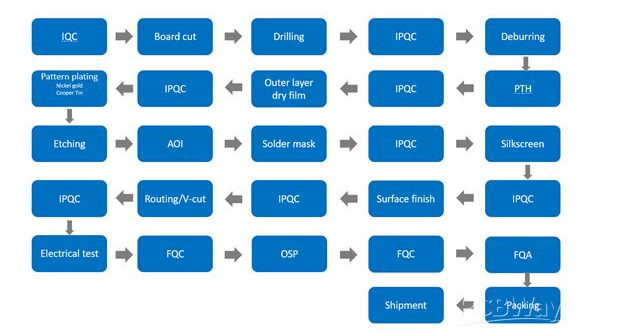
PCB Fabrication Process
1. Substrate Preparation
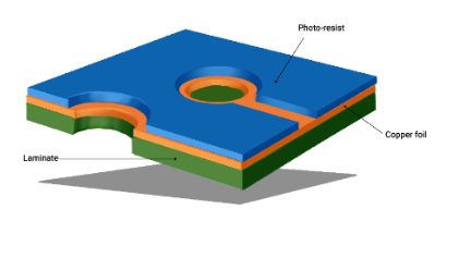
The fabrication process begins with the selection and preparation of the substrate material. Most standard PCBs use FR-4, a glass-reinforced epoxy laminate. The substrate is cleaned and coated with a thin layer of copper on one or both sides, depending on the board design.
2. Patterning (Photolithography)
The copper-clad substrate undergoes photolithography to transfer the circuit pattern:
- Photoresist Application: A light-sensitive chemical (photoresist) is applied to the copper surface
- Exposure: UV light passes through a photomask containing the circuit pattern, hardening the exposed photoresist
- Development: The unexposed photoresist is washed away, leaving the desired pattern
3. Etching
The board is immersed in an etching solution (typically ammonium persulfate or ferric chloride) that removes unprotected copper, leaving only the desired circuit traces protected by hardened photoresist.
4. Drilling
Precision drilling creates holes for through-hole components and vias. Modern PCB fabrication uses computer-controlled drilling machines with carbide drill bits capable of creating holes as small as 100 microns in diameter.
5. Plating and Copper Deposition
Holes are plated with copper to establish electrical connections between layers in multilayer boards. This process typically involves:
- Electroless copper deposition to create a conductive base layer
- Electroplating to build up the copper thickness
- Additional plating may include tin, gold, or other metals for specific applications
6. Solder Mask Application
A protective solder mask is applied over the entire board except for areas requiring soldering. This layer:
- Prevents solder bridges between closely spaced pads
- Protects copper traces from oxidation
- Provides electrical insulation
- Enhances the board’s aesthetic appearance
7. Silkscreen Printing
The final fabrication step applies component designators, logos, and other markings using epoxy ink. This silkscreen layer aids in assembly and troubleshooting.
8. Surface Finishing
Various surface finishes may be applied to exposed copper areas:
- HASL (Hot Air Solder Leveling): Traditional lead or lead-free solder coating
- ENIG (Electroless Nickel Immersion Gold): Provides excellent solderability and shelf life
- OSP (Organic Solderability Preservative): Cost-effective temporary protection
- Immersion Silver/Tin: Alternative finishes for specific applications
PCB Assembly Processes
With the bare board fabricated, the assembly process begins to populate the PCB with electronic components.
1. Solder Paste Application
For surface mount technology (SMT) components, solder paste is precisely deposited on pads using a stencil printing process. The stencil, typically made of stainless steel, aligns perfectly with the PCB to ensure accurate paste deposition.
2. Component Placement
Modern assembly lines use automated pick-and-place machines that can place thousands of components per hour with micron-level precision. These machines:
- Retrieve components from reels or trays
- Orient them correctly
- Place them on the solder paste with exact positioning
3. Reflow Soldering
The populated board passes through a reflow oven with precisely controlled temperature zones:
- Preheat: Gradually raises the board temperature to activate flux
- Soak: Allows temperature stabilization across the board
- Reflow: Exceeds solder melting point (typically 217-250°C for lead-free)
- Cooling: Solidifies joints while minimizing thermal stress
4. Through-Hole Component Assembly
For through-hole components, two primary methods exist:
- Wave Soldering: The board passes over a molten solder wave that wicks into plated through-holes
- Manual Soldering: Used for prototypes, rework, or large components
5. Conformal Coating (Optional)
Some assemblies receive a protective conformal coating to:
- Prevent moisture ingress
- Protect against contaminants
- Provide additional insulation
- Enhance mechanical stability
6. Inspection and Testing
Quality control is critical throughout the assembly process:
- Automated Optical Inspection (AOI): Cameras verify component presence, orientation, and solder quality
- X-ray Inspection: Examines hidden joints like BGA connections
- In-Circuit Testing (ICT): Electrical tests verify proper connections and component values
- Functional Testing: Validates the complete assembly under operational conditions
Advanced PCB Technologies
Modern electronics demand increasingly sophisticated PCB solutions:
1. High-Density Interconnect (HDI) PCBs
Feature finer lines/spaces (<100μm), smaller vias, and higher connection pad densities to accommodate complex IC packages.
2. Flexible and Rigid-Flex PCBs
Use polyimide or other flexible materials for applications requiring bending or dynamic flexing.
3. High-Frequency PCBs
Employ specialized materials (PTFE, ceramic-filled) with carefully controlled dielectric properties for RF/microwave applications.
4. Embedded Component PCBs
Incorporate passive components within the board layers to save space and improve performance.
Quality Standards and Certifications
Reputable PCB manufacturers adhere to various quality standards:
- IPC-A-600: Acceptability of Printed Boards
- IPC-A-610: Acceptability of Electronic Assemblies
- ISO 9001: Quality Management Systems
- UL Certification: Safety standards compliance
- RoHS/REACH: Environmental compliance
Challenges in PCB Fabrication and Assembly
The industry faces several ongoing challenges:
- Miniaturization: Shrinking component sizes demand higher precision
- Material Costs: Fluctuating prices for copper and specialty substrates
- Environmental Regulations: Compliance with evolving chemical restrictions
- Supply Chain Issues: Component shortages affecting assembly timelines
- Thermal Management: Dissipating heat from increasingly powerful devices
Future Trends in PCB Technology
Several emerging technologies are shaping the future of PCB fabrication and assembly:
- Additive Manufacturing: 3D printing of conductive traces and dielectric materials
- Embedded Active Components: Integration of semiconductor devices within PCB layers
- Advanced Materials: Nanocomposites and graphene-based conductors
- AI-Driven Design: Machine learning optimizing layouts for performance and manufacturability
- Sustainable Practices: Increased recycling and reduced chemical usage
Conclusion
PCB fabrication and assembly represent a complex, precision-driven manufacturing process that continues to evolve alongside technological advancements. From simple single-layer boards to sophisticated multilayer HDI designs, the industry constantly adapts to meet the demands of modern electronics. Understanding these processes is essential for designers, engineers, and procurement professionals working with electronic products.
As we look toward the future, PCB technology will undoubtedly continue its trajectory toward higher densities, improved performance, and greater integration—enabling the next generation of electronic innovations that will transform our world.