PCB Edge Plating: Techniques, Benefits, and Design Considerations
Introduction to PCB Edge Plating
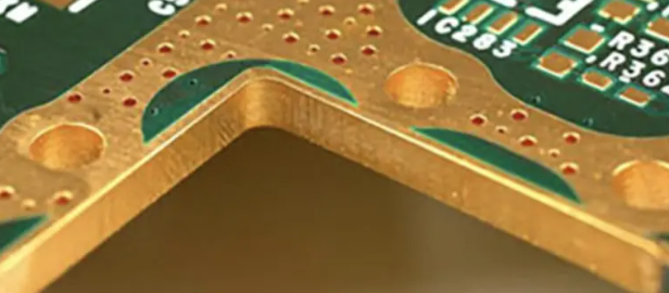
Printed Circuit Board (PCB) edge plating, also known as board edge plating or castellation, is a specialized manufacturing process that involves depositing a conductive metal layer along the perimeter edges of a PCB. This technique serves multiple purposes in modern electronics design, ranging from improved electromagnetic shielding to enhanced mechanical connections.
Edge plating has become increasingly important as electronic devices continue to shrink in size while demanding higher performance. The technology enables designers to create more robust interconnections, better shielding solutions, and more reliable PCB assemblies in space-constrained applications.
This article will explore the various aspects of PCB edge plating, including its manufacturing processes, key benefits, design considerations, and common applications in today’s electronics industry.
Manufacturing Process of PCB Edge Plating
1. Pre-processing Steps
The edge plating process begins with standard PCB fabrication up to the point where the board profile is routed. Before plating can occur, several preparatory steps must be completed:
- Routing/Scoring: The PCB outline is created using either routing or scoring methods, leaving a clean edge surface
- Deburring: Any rough edges or imperfections are removed to ensure uniform plating
- Cleaning: The edge surfaces undergo thorough cleaning to remove contaminants that could affect plating adhesion
- Micro-etching: A mild chemical etch creates microscopic roughness for better mechanical bonding of the plated metal
2. Electroless Copper Deposition
The actual plating process typically starts with electroless copper deposition:
- Catalyst Application: A palladium-based catalyst is applied to prepare the surface for copper deposition
- Electroless Copper: A thin layer (0.5-2μm) of copper is chemically deposited on all exposed surfaces, including the edges
- Quality Check: The uniformity of the electroless copper layer is verified before proceeding
3. Pattern Plating
For selective edge plating (rather than plating the entire edge), a dry film resist is applied and patterned:
- Lamination: Dry film resist is laminated over the entire board
- Exposure: UV light exposes the resist through a photomask defining the plating areas
- Development: Unexposed resist is removed, leaving the desired plating pattern
4. Electrolytic Plating
The main conductive layer is added through electrolytic plating:
- Copper Plating: Typically 20-25μm of copper is electroplated onto the electroless copper layer
- Additional Metals: Optional layers like nickel (3-5μm) and gold (0.05-0.1μm) may be added for specific applications
- Resist Stripping: The dry film resist is removed after plating completion
5. Final Processing
The completed edge plating undergoes final treatments:
- Etching: Any unwanted copper is removed from non-plated areas
- Surface Finishing: Additional surface treatments like immersion silver or ENIG may be applied
- Quality Inspection: Plating thickness, adhesion, and continuity are verified
Benefits of PCB Edge Plating
1. Enhanced Electromagnetic Compatibility (EMC)
Edge plating significantly improves a PCB’s EMC performance:
- Faraday Cage Effect: When connected to ground on multiple layers, edge plating creates a partial Faraday cage around the PCB
- Reduced Radiation: Containing electromagnetic fields within the board reduces unwanted emissions
- Improved Immunity: The shielding protects sensitive circuits from external interference
- Lower Crosstalk: Edge plating can minimize coupling between adjacent boards in stacked configurations
2. Improved Mechanical Strength
The metal plating reinforces the PCB structure:
- Edge Protection: Plating prevents delamination and fiber exposure at board edges
- Impact Resistance: The metal layer helps withstand physical shocks and vibrations
- Moisture Barrier: Reduces moisture ingress through the board edges
- Increased Durability: Extends the PCB’s lifespan in harsh environments
3. Enhanced Electrical Connectivity
Edge plating creates reliable electrical connections:
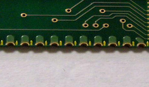
- Edge Connectors: Enables reliable edge card connections without separate connectors
- Inter-board Connections: Facilitates direct board-to-board connections in stacked assemblies
- Low Resistance Path: Provides high-current capable connections between board sides
- Grounding: Offers excellent grounding points for chassis or shield connections
4. Design Flexibility
Edge plating enables innovative PCB designs:
- 3D Packaging: Supports complex multi-board assemblies
- Space Savings: Eliminates need for separate connectors in tight spaces
- Aesthetic Appeal: Provides a professional, finished look to board edges
- Custom Shapes: Allows plating of complex edge profiles including cutouts
Design Considerations for PCB Edge Plating
1. Layout Guidelines
Proper design is crucial for successful edge plating implementation:
- Plating Width: Typically 0.5-2mm from the edge, depending on application
- Layer Connections: Ensure solid connections to internal ground/power planes
- Clearance: Maintain adequate spacing between plated edges and nearby traces
- Corner Design: Use rounded corners (≥0.5mm radius) for more reliable plating
2. Material Selection
Choice of materials affects plating quality and performance:
- Base Material: FR-4 is most common, but high-frequency materials may require special treatment
- Copper Weight: 1oz (35μm) base copper is typical, but heavier copper may be needed for high current
- Surface Finish: ENIG, immersion silver, or gold plating depending on application needs
- Solder Mask: Should be kept back from plated edges (typically 0.1-0.2mm)
3. Manufacturing Constraints
Design must account for fabrication limitations:
- Minimum Plating Width: Typically 0.3mm for reliable plating
- Aspect Ratio: Plating depth-to-width ratio affects plating uniformity
- Tooling Holes: Required for proper alignment during plating process
- Panelization: May require special consideration for depaneling after plating
4. Reliability Factors
Design choices impact long-term reliability:
- Thermal Expansion: Account for CTE differences between copper and substrate
- Mechanical Stress: Avoid sharp transitions that could concentrate stress
- Corrosion Protection: Specify appropriate finishes for the operating environment
- Adhesion Promoters: May be needed for certain substrate materials
Applications of PCB Edge Plating
1. High-Frequency/RF Circuits
Edge plating is particularly valuable in RF applications:
- Antenna Modules: Provides controlled grounding and shielding
- RF Shields: Creates effective cavity shielding when combined with covers
- Microwave Circuits: Minimizes parasitic radiation and interference
- 5G Devices: Essential for millimeter-wave frequency boards
2. Industrial Electronics
Harsh environment applications benefit from edge plating:
- Motor Drives: Provides EMI shielding and robust edge protection
- Power Supplies: Offers low-impedance grounding paths
- Control Systems: Enhances reliability in vibration-prone installations
- Outdoor Equipment: Protects against moisture and contamination
3. Consumer Electronics
Space-constrained consumer devices utilize edge plating:
- Smartphones: Enables compact board-to-board connections
- Wearables: Provides durable edges in miniature PCBs
- IoT Devices: Offers both shielding and connection solutions
- Gaming Hardware: Supports high-speed edge connectors
4. Automotive Electronics
Automotive applications demand the reliability of edge plating:
- ECUs: Protects against under-hood environmental challenges
- Infotainment: Shields sensitive audio/video circuits
- ADAS: Ensures reliable operation of safety-critical systems
- LED Lighting: Provides robust connections in compact designs
Challenges and Solutions in PCB Edge Plating
1. Plating Uniformity
Maintaining consistent plating thickness can be challenging:
- Solution: Optimize racking design and current distribution
- Solution: Use pulse plating techniques for better thickness control
- Solution: Implement proper pre-treatment processes
2. Adhesion Issues
Plating delamination is a common reliability concern:
- Solution: Ensure proper surface preparation and micro-etching
- Solution: Use adhesion promoters for difficult substrates
- Solution: Specify appropriate copper roughness parameters
3. Cost Considerations
Edge plating adds to fabrication costs:
- Solution: Use selective plating only where needed
- Solution: Design for panel efficiency to maximize throughput
- Solution: Balance performance needs with cost constraints
4. Depaneling Challenges
Separating plated boards requires special care:
- Solution: Use routing instead of scoring for plated edges
- Solution: Design breakaway tabs with plating clearance
- Solution: Specify appropriate depaneling methods with fabricator
Future Trends in PCB Edge Plating Technology
1. Advanced Materials
Emerging materials are influencing edge plating development:
- Low-Loss Substrates: New dielectric materials require adapted plating processes
- Nanocomposite Coatings: May offer enhanced edge protection alternatives
- Conductive Polymers: Potential for hybrid plating approaches
2. Miniaturization
Continuing size reduction drives innovation:
- Micro-edge Plating: Techniques for ultra-narrow edge plating
- 3D Packaging: Edge plating for chip-scale PCB assemblies
- High-Density Interconnects: Finer pitch edge connections
3. Sustainable Processes
Environmental considerations are shaping future developments:
- Reduced Chemical Processes: Development of more eco-friendly plating chemistries
- Waste Minimization: Improved process efficiency and recycling
- Alternative Materials: Exploration of less toxic plating options
4. Smart Integration
Edge plating may enable new functionalities:
- Embedded Sensors: Plated edges with sensing capabilities
- Thermal Management: Enhanced edge cooling solutions
- Optoelectronic Integration: Combined electrical/optical edge interfaces
Conclusion
PCB edge plating has evolved from a niche manufacturing technique to an essential technology in modern electronics design. Its ability to provide electromagnetic shielding, enhance mechanical robustness, and enable innovative interconnection solutions makes it invaluable across numerous applications from consumer devices to industrial systems.
As electronic devices continue advancing toward higher frequencies, greater miniaturization, and increased reliability requirements, edge plating technologies will continue to develop in response. Designers who master the principles and best practices of edge plating implementation will be better equipped to meet these evolving challenges.
Successful edge plating implementation requires close collaboration between design engineers and PCB fabricators, with careful attention to material selection, layout optimization, and manufacturing process capabilities. When properly executed, edge plating can significantly enhance PCB performance and reliability while enabling more compact and cost-effective electronic assemblies.
The future of edge plating lies in the development of more advanced materials, more precise manufacturing techniques, and innovative applications that leverage the unique benefits of plated edges. As these advancements emerge, edge plating will undoubtedly play an even greater role in next-generation electronic designs.