PCB Solder Mask Material: Composition, Types, and Selection Criteria
Introduction to Solder Mask Materials
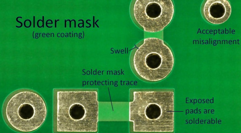
Printed Circuit Board (PCB) solder mask, also known as solder resist or solder stop mask, is a thin lacquer-like layer of polymer applied to the copper traces of a PCB. This critical material serves multiple purposes in modern electronics manufacturing, providing both physical protection and electrical insulation. The solder mask prevents solder bridges from forming between closely spaced solder pads during the assembly process while protecting the copper circuitry from oxidation and environmental damage.
The evolution of solder mask materials has paralleled the advancement of PCB technology. Early circuit boards often went without solder mask, but as component density increased and trace spacing decreased, the need for precise solder control became essential. Today, solder mask is an indispensable part of PCB fabrication, with material formulations specifically engineered to meet the demands of various applications from consumer electronics to aerospace systems.
Composition of Solder Mask Materials
Modern solder mask materials are complex formulations designed to provide specific performance characteristics. The typical composition includes:
Resin Systems
The resin forms the matrix of the solder mask and determines many of its fundamental properties. Epoxy resins are most common due to their excellent adhesion, chemical resistance, and thermal stability. Acrylic resins offer different curing characteristics and are often used in photoimageable solder masks. More specialized formulations may use polyimide or silicone resins for extreme temperature applications.
Pigments and Dyes
Solder masks incorporate pigments to provide color (most commonly green, but also available in red, blue, black, yellow, and white) and opacity. The pigments must withstand soldering temperatures without degradation. Titanium dioxide is frequently used for white masks, while phthalocyanine compounds provide the classic PCB green.
Photoinitiators
In photoimageable solder masks, photoinitiators are crucial components that enable the patterning process. These compounds generate free radicals or acids when exposed to specific wavelengths of light (typically UV), initiating the cross-linking reaction that cures the exposed areas of the mask.
Solvents
Solvents maintain the solder mask in liquid form for application, then evaporate during pre-cure baking (known as the “soft bake” or “tack dry” stage). The choice of solvent affects application properties, drying characteristics, and environmental considerations.
Additives
Various additives modify the properties of the solder mask:
- Fillers improve thermal and mechanical properties
- Flow control agents regulate viscosity and surface tension
- Adhesion promoters enhance bonding to copper and substrate
- Stabilizers prevent premature curing or degradation
Types of Solder Mask Materials
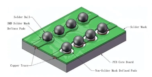
Liquid Photoimageable Solder Masks (LPSM)
Liquid Photoimageable Solder Masks dominate the PCB industry due to their excellent resolution and process flexibility. Applied by screen printing or curtain coating, these masks are dried to a tack-free state, then exposed through a photomask and developed to remove unexposed areas. LPSMs offer:
- High resolution (typically 50-75μm)
- Excellent adhesion to copper and substrate
- Good chemical and thermal resistance
- Relatively low cost compared to dry films
Dry Film Solder Masks (DFSM)
Dry Film Solder Masks come as pre-formed sheets laminated onto the PCB under heat and pressure. While less common than liquid masks, they offer some distinct advantages:
- Superior thickness uniformity
- Excellent coverage over uneven surfaces
- No solvent evaporation concerns
- Good for fine pitch applications
However, DFSMs generally have lower resolution than liquid masks and higher material costs.
Thermal Cure Solder Masks
These non-photoimageable masks cure entirely through heat and are typically applied by screen printing. While less precise than photoimageable versions, they’re suitable for:
- Low-cost, high-volume production
- Boards with less demanding feature sizes
- Applications where UV equipment isn’t available
UV Cure Solder Masks
Curing rapidly under UV light, these masks offer fast processing times but may have limitations in:
- Depth of cure (thick coatings may cure incompletely)
- Long-term thermal stability
- Adhesion on certain surfaces
They’re often used for quick-turn prototypes or repair work.
Specialty Solder Masks
Various specialized formulations address particular needs:
- Flexible solder masks for flex and rigid-flex PCBs use elastomeric resins
- High-temperature masks withstand repeated lead-free soldering cycles
- Low-Dk masks minimize dielectric constant for high-frequency applications
- Tenting masks provide extra thickness for via protection
Properties and Performance Characteristics
Thermal Properties
Solder masks must endure multiple soldering cycles (typically 260°C for lead-free processes) without degradation. Key thermal characteristics include:
- Glass Transition Temperature (Tg): The temperature at which the polymer transitions from glassy to rubbery state
- Thermal Decomposition Temperature: When chemical breakdown begins
- Coefficient of Thermal Expansion (CTE): Should match the PCB substrate to prevent delamination
Electrical Properties
While primarily an insulator, solder mask affects circuit performance:
- Dielectric Strength: Typically 500-1000 V/mil
- Surface Insulation Resistance (SIR): Measures resistance to electrical leakage
- Dielectric Constant (Dk): Usually 3.5-4.5 at 1 MHz
- Dissipation Factor (Df): Typically 0.02-0.04 at 1 MHz
Mechanical Properties
- Adhesion Strength: Measured by peel tests, typically 4-8 N/cm
- Pencil Hardness: Indicates scratch resistance, usually 4H-6H
- Flexibility: Critical for flex circuits, measured by mandrel bend tests
Chemical Resistance
Solder masks must resist:
- Flux chemicals during assembly
- Cleaning solvents
- Environmental contaminants
- Moisture absorption (typically <2%)
Application Processes
Surface Preparation
Proper surface preparation ensures good adhesion:
- Cleaning: Removes oxides and contaminants
- Microetching: Creates a roughened surface for mechanical bonding
- Pre-treatment: Some processes use chemical promoters
Application Methods
- Screen Printing: Traditional method using emulsion screens
- Good for simple designs
- Lower resolution (~100μm)
- Cost-effective for high volumes
- Curtain Coating: Flows mask over the board in a controlled curtain
- Excellent for high-volume production
- Good thickness uniformity
- Limited to flat boards
- Spray Coating: Atomized application
- Good for irregular surfaces
- Allows variable thickness
- Requires masking of keep-out areas
- Electrostatic Spray: Charged particles improve transfer efficiency
- Reduced material waste
- Excellent coverage
- Requires specialized equipment
- Lamination (for dry film): Heat and pressure application
- No drying step required
- Excellent thickness control
- Higher material cost
Imaging and Development
For photoimageable masks:
- Pre-bake (Drying): Removes solvents, typically 70-80°C
- Exposure: UV light through phototool, 100-400 mJ/cm²
- Development: Removes unexposed areas with aqueous or solvent chemistry
- Post-bake (Final Cure): Completes polymerization, 140-160°C
Selection Criteria for Solder Mask Materials
Technical Requirements
- Feature Resolution: LPSM for <75μm features
- Board Type: Flex circuits need flexible chemistries
- Soldering Process: Lead-free requires higher temperature resistance
- Environmental Conditions: Harsh environments may need specialty masks
Manufacturing Considerations
- Curing Equipment Available: UV vs. thermal capabilities
- Process Compatibility: Must work with existing production flow
- Throughput Requirements: Some cure faster than others
Cost Factors
- Material Cost: Dry films typically more expensive
- Application Efficiency: Waste in different processes
- Yield Impact: Higher performance masks may reduce defects
Regulatory Compliance
- UL Recognition: Important for safety-critical applications
- RoHS Compliance: Free of restricted substances
- Halogen-Free Requirements: For some environmental standards
Recent Developments and Future Trends
Advanced Formulations
- Low-loss materials for 5G and high-frequency applications
- Thermally conductive masks for better heat dissipation
- Self-healing materials that repair minor damage
Application Innovations
- Inkjet printing for digital patterning without phototools
- 3D mask application for complex board geometries
- Selective coating systems for hybrid protection schemes
Environmental Initiatives
- Water-developable masks reducing solvent use
- Bio-based resins from renewable sources
- Low-VOC formulations improving workplace safety
Enhanced Performance
- Higher temperature resistance for emerging soldering technologies
- Improved adhesion for high-reliability applications
- Better optical properties for automated inspection
Conclusion
PCB solder mask materials have evolved from simple protective coatings to sophisticated engineered materials that actively contribute to board performance and reliability. The selection of appropriate solder mask involves careful consideration of technical requirements, manufacturing processes, and cost factors. As electronics continue advancing toward higher densities, higher frequencies, and more demanding environments, solder mask technology will continue evolving to meet these challenges. Future developments will likely focus on materials that enable finer features, withstand higher processing temperatures, and comply with increasingly stringent environmental regulations—all while maintaining or reducing overall production costs. Understanding the composition, properties, and application methods of various solder mask materials empowers PCB designers and manufacturers to make informed decisions that optimize both performance and manufacturability.