Optimizing PCBA Processes for Enhanced PCB Performance
Key Takeaways
Effective PCB assembly requires a systematic approach to optimize both design and manufacturing stages. Implementing PCBA best practices ensures higher reliability, particularly when addressing thermal management and component placement. Key strategies include:
| Optimization Focus | Impact on Performance |
|---|---|
| Precision Soldering | Reduces risk of cold joints |
| Automated Testing | Enhances defect detection rates |
| Material Selection | Improves thermal/mechanical stability |
Tip: Prioritize design-for-manufacturability (DFM) checks during prototyping to minimize rework in printed circuit board assembly.
Critical quality controls, such as automated optical inspection (AOI) and X-ray testing, are indispensable for identifying latent defects in PCBA systems. For instance, advanced testing protocols can detect micro-cracks in solder joints, which are often invisible during manual inspections.
Additionally, refining reflow soldering profiles and adopting lead-free soldering materials align with industry sustainability standards while maintaining PCB reliability. Process streamlining, such as reducing component-to-board distance, directly enhances signal integrity and thermal dissipation.
By integrating these techniques, manufacturers achieve fault-tolerant designs and faster time-to-market—critical for high-performance applications like aerospace or medical devices.
PCBA Process Optimization for Superior PCB Reliability
Achieving superior PCB reliability begins with meticulous optimization of PCBA (Printed Circuit Board Assembly) processes. Modern PCB assembly workflows demand precise coordination between design, material selection, and manufacturing techniques to mitigate risks such as thermal stress, solder joint fractures, or signal integrity issues. For instance, optimizing component placement to minimize trace lengths reduces electromagnetic interference (EMI), while advanced solder paste stenciling techniques ensure consistent deposition for reliable electrical connections.
A critical focus area is the integration of automated optical inspection (AOI) systems, which enhance defect detection during PCBA stages. Pairing AOI with X-ray inspection for hidden joints in ball grid array (BGA) components further strengthens quality assurance. Additionally, implementing controlled reflow profiles tailored to specific PCB materials prevents warping or delamination, directly impacting long-term durability.
Process refinements also extend to environmental controls, where humidity and temperature stabilization during PCB assembly curbs moisture absorption—a key factor in electrochemical migration. For deeper insights into foundational PCB design principles, refer to this comprehensive guide.
By aligning PCBA workflows with design-for-manufacturability (DFM) guidelines and leveraging real-time data analytics, manufacturers can systematically eliminate variability, ensuring each circuit board meets stringent reliability benchmarks. This holistic approach not only reduces failure rates but also streamlines compliance with industry standards like IPC-A-610.
Key Assembly Techniques to Enhance Circuit Board Efficiency
Achieving peak efficiency in PCB assembly requires precision-driven methodologies that align with modern manufacturing demands. One critical approach involves optimizing surface-mount technology (SMT) placement, where automated pick-and-place systems ensure micron-level accuracy for component alignment. This minimizes signal interference and reduces thermal stress, directly improving PCBA reliability. Additionally, incorporating laser-cut stencils for solder paste application enhances deposition consistency, which is vital for preventing defects like bridging or insufficient joints.
Another essential practice is implementing design for manufacturability (DFM) principles early in the PCB assembly process. By collaborating with design engineers to adjust pad geometries or component spacing, manufacturers can streamline assembly workflows and mitigate rework risks. For high-density boards, sequential lamination techniques help manage layer alignment, ensuring impedance control and signal integrity in complex PCBA systems.
Transitioning to closed-loop process monitoring further elevates efficiency. Real-time feedback systems track variables such as solder temperature and conveyor speed, enabling immediate adjustments to maintain PCBA quality standards. Pairing this with rigorous automated optical inspection (AOI) ensures defects are identified before downstream testing phases, reducing cycle times and material waste.
By integrating these techniques, manufacturers can balance speed and precision, delivering PCB assembly outputs that meet both performance benchmarks and cost-efficiency targets.
Implementing Quality Controls in PCB Assembly Processes
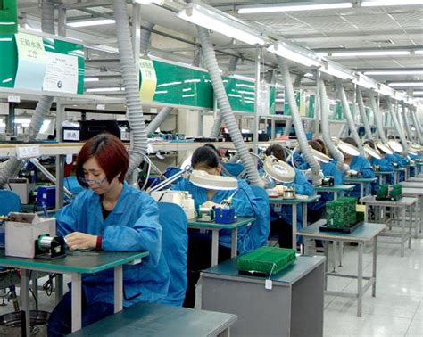
Effective PCB assembly relies on rigorous quality control protocols to ensure consistent performance and longevity of PCBA systems. Automated optical inspection (AOI) serves as a foundational step, identifying defects like misaligned components or insufficient solder joints early in production. Pairing AOI with X-ray inspection enhances detection of hidden flaws, particularly in high-density or multilayer boards.
Material verification is equally critical. Testing solder paste viscosity and composition prevents issues such as cold joints or bridging, which compromise PCB assembly reliability. Implementing statistical process control (SPC) tools enables real-time monitoring of key parameters, ensuring deviations are corrected before they escalate.
For mission-critical applications, environmental stress testing—including thermal cycling and vibration analysis—validates PCBA durability under operational extremes. Partnering with certified suppliers, like Kingstec’s PCB assembly services, ensures adherence to international standards such as IPC-A-610 and ISO 9001.
Finally, traceability systems embedded in PCB assembly workflows document each production stage, simplifying root-cause analysis for post-deployment failures. By integrating these layered controls, manufacturers reduce rework costs while elevating end-product consistency—a prerequisite for industries demanding zero-defect PCBA outputs.
Advanced Testing Methods for High-Performance PCBA Systems
Ensuring the reliability of PCBA systems demands rigorous testing protocols tailored to modern electronics’ complexity. Advanced testing methodologies such as Automated Optical Inspection (AOI) and X-Ray Inspection are indispensable for identifying microscopic defects like solder bridging or component misalignment. These tools enable manufacturers to scrutinize PCB assembly layers non-destructively, preserving integrity while detecting flaws invisible to manual inspection.
For high-frequency or mission-critical applications, In-Circuit Testing (ICT) validates electrical performance by measuring resistance, capacitance, and signal continuity across circuits. Complementing this, functional testing simulates real-world operating conditions to verify that the PCBA behaves as intended under load. Environmental stress screening, including thermal cycling and vibration tests, further ensures durability in harsh conditions.
Integrating Design for Testability (DFT) principles early in the PCB assembly process minimizes post-production bottlenecks. By embedding test points and leveraging boundary-scan techniques, engineers streamline diagnostics without compromising board layout. Partnering with specialized providers like CE3 Electronics can enhance access to cutting-edge testing infrastructure, ensuring compliance with industry standards like IPC-A-610.
As PCBA systems grow denser, combining automated diagnostics with AI-driven anomaly detection becomes critical. These innovations not only accelerate defect identification but also reduce false positives, aligning with the broader goal of optimizing manufacturing efficiency while maintaining stringent quality benchmarks.
Streamlining PCB Assembly for Maximum Operational Efficiency
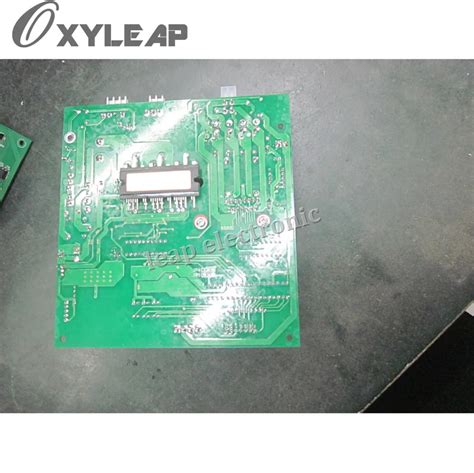
Achieving peak efficiency in PCB assembly requires a systematic approach to process optimization. By integrating automated pick-and-place systems and high-precision soldering technologies, manufacturers can reduce cycle times while maintaining stringent quality standards. A key strategy involves adopting surface-mount technology (SMT) for densely populated boards, which minimizes manual intervention and enhances repeatability.
Workflow analysis tools, such as value stream mapping, help identify bottlenecks in PCBA production lines, enabling targeted improvements like parallel processing or modular workstation designs. For instance, synchronizing solder paste application with component placement reduces idle time by up to 30%, as noted in recent studies on printed circuit board manufacturing.
Additionally, implementing real-time monitoring systems ensures immediate detection of defects, preventing costly rework. Advanced thermal profiling during reflow soldering further optimizes energy use and mitigates warping risks. By balancing automation with data-driven adjustments, manufacturers can streamline PCB assembly workflows to achieve consistent output quality and scalable throughput—critical for meeting evolving industry demands.
Critical Design Considerations for Reliable PCBA Production
Achieving consistent reliability in PCBA manufacturing demands meticulous attention to design parameters that influence both functionality and longevity. A foundational step involves optimizing PCB assembly layouts to minimize electromagnetic interference (EMI) and ensure proper signal integrity. Component placement, for instance, must balance spatial efficiency with thermal management, as clustered components can create hotspots that degrade performance.
Material selection plays a pivotal role, particularly in high-frequency or high-temperature applications. Substrates with low thermal expansion coefficients and copper layers with adequate thickness help prevent warping or trace fractures during thermal cycling. Additionally, designers should prioritize PCB assembly-friendly footprints, ensuring components align with automated placement systems to reduce errors during soldering.
Trace routing requires careful planning to avoid crosstalk and impedance mismatches. Implementing controlled impedance routing and adhering to industry-standard clearance rules mitigate short-circuit risks. For multilayer boards, stack-up configurations must account for power plane stability and signal layer isolation.
Finally, integrating Design for Manufacturing (DFM) and Design for Testing (DFT) guidelines early in the process streamlines PCBA validation. Test points should be accessible for in-circuit testing (ICT), while fiducial markers enhance alignment accuracy during assembly. By addressing these factors holistically, manufacturers can preempt defects and elevate the reliability of finished PCBA systems.
Optimizing Soldering Processes to Prevent PCB Failures
Effective PCB assembly relies heavily on refining soldering techniques to mitigate risks of circuit board malfunctions. In PCBA manufacturing, even minor defects in solder joints—such as cold joints, bridging, or voids—can compromise electrical connectivity and long-term reliability. To address this, manufacturers prioritize precise control of reflow soldering profiles, ensuring optimal thermal gradients to prevent component stress while achieving uniform alloy formation. For wave soldering applications, adjusting preheat temperatures and conveyor speeds minimizes thermal shock to sensitive components.
Advanced inspection tools like automated optical inspection (AOI) and X-ray imaging are critical for identifying microscopic flaws in solder connections post-assembly. Additionally, adopting nitrogen-assisted soldering reduces oxidation, enhancing joint integrity in high-density PCBA designs. Process consistency is further improved by monitoring solder paste viscosity and stencil alignment during screen printing, which directly impacts deposition accuracy.
By integrating these strategies, PCB assembly teams reduce failure rates caused by soldering inconsistencies, ensuring boards meet stringent performance benchmarks. This focus on precision not only extends product lifespans but also aligns with broader goals of optimizing PCBA workflows for efficiency and reliability.
Essential Process Refinements for Efficient PCB Manufacturing
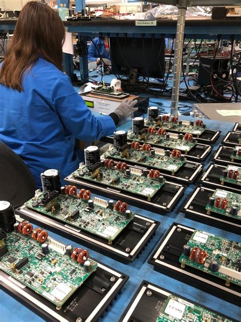
Achieving peak efficiency in PCB assembly requires meticulous attention to process refinements that align with modern manufacturing demands. A critical starting point is optimizing automation workflows to reduce manual intervention, minimizing human error while accelerating production timelines. For instance, integrating precision pick-and-place systems ensures accurate component positioning during PCBA, directly enhancing board reliability.
Another key refinement involves thermal management during soldering. By calibrating reflow ovens to maintain consistent temperature profiles—tailored to specific component tolerances—manufacturers can prevent defects like cold joints or delamination. Pairing this with real-time monitoring tools allows immediate adjustments, ensuring adherence to quality benchmarks.
Material selection also plays a pivotal role. Using high-quality substrates and solder alloys compatible with PCB assembly environments improves signal integrity and thermal resilience. Additionally, adopting design-for-manufacturability (DFM) principles early in the design phase reduces rework by addressing potential assembly challenges, such as component spacing or pad alignment.
Finally, streamlining post-assembly testing protocols, such as automated optical inspection (AOI) and in-circuit testing (ICT), ensures defects are identified before boards enter high-value stages. These refinements collectively elevate PCBA efficiency, bridging the gap between theoretical design and real-world performance.
Conclusion
In the evolving landscape of electronics manufacturing, optimizing PCBA processes remains pivotal to achieving peak performance in PCB assembly. By integrating advanced testing protocols, precision-driven soldering techniques, and robust quality controls, manufacturers can significantly enhance the reliability and longevity of circuit boards. A holistic approach—spanning design validation, material selection, and process automation—ensures that PCBA systems meet stringent operational demands while minimizing defects.
The interplay between thermal management and signal integrity underscores the importance of iterative refinements in PCB assembly workflows. Proactive identification of failure modes, coupled with data-driven process adjustments, fosters efficiency gains across production cycles. Ultimately, the synergy of these strategies not only elevates PCBA outcomes but also positions manufacturers to adapt swiftly to emerging technological challenges. By prioritizing continuous improvement, stakeholders can unlock new thresholds of performance in modern electronics ecosystems.
FAQs
What distinguishes PCB assembly from PCBA in manufacturing?
PCB assembly refers to the process of populating a bare circuit board with components, while PCBA (Printed Circuit Board Assembly) encompasses the complete process, including soldering, testing, and quality validation. Optimizing both stages ensures reliability and performance in final products.
How do quality controls impact PCBA outcomes?
Robust quality controls, such as Automated Optical Inspection (AOI) and X-ray testing, identify defects like solder bridges or misaligned components early. These measures reduce failure rates and align with PCB assembly standards for high-volume production.
What design factors influence PCBA efficiency?
Component placement, thermal management, and trace routing directly affect assembly speed and functionality. Designs optimized for PCBA minimize rework and enhance signal integrity, particularly in high-frequency applications.
Why is soldering critical for PCB reliability?
Inconsistent soldering techniques can lead to cold joints or shorts, compromising long-term durability. Advanced methods like reflow soldering and selective soldering ensure precise connections, vital for complex PCBA systems.
How can manufacturers streamline PCB assembly workflows?
Adopting automated pick-and-place systems and real-time process monitoring reduces human error and cycle times. Pairing these with predictive maintenance further enhances operational efficiency in PCBA production.
Ready to Elevate Your PCBA Workflow?
For expert guidance on optimizing your PCB assembly processes, please click here to explore tailored solutions at https://www.andwinpcb.com/pcb-assembly/.


