PCB Transformers: Design, Applications, and Future Trends
Introduction to PCB Transformers
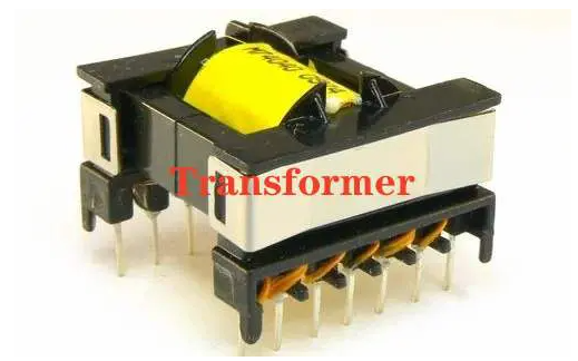
Printed Circuit Board (PCB) transformers represent a significant advancement in transformer technology, offering compact, lightweight, and highly integrable solutions for modern electronic applications. Unlike conventional wire-wound transformers, PCB transformers are fabricated directly onto printed circuit boards using copper traces as windings, creating a more streamlined and manufacturable component.
PCB transformers operate on the same fundamental principles of electromagnetic induction as traditional transformers but achieve this through planar rather than cylindrical windings. This innovative approach provides numerous advantages in terms of size reduction, repeatable manufacturing, thermal performance, and integration with other electronic components.
The development of PCB transformers has been driven by the continuous miniaturization of electronic devices and the growing demand for power electronics solutions that can be mass-produced with high consistency. These transformers find applications across various industries, from consumer electronics to automotive systems and renewable energy technologies.
Fundamental Principles of PCB Transformers
Basic Operating Principles
PCB transformers function based on Faraday’s law of electromagnetic induction, where alternating current in the primary winding creates a time-varying magnetic field that induces voltage in the secondary winding. The key difference lies in the physical implementation—instead of using round wires wound around a core, PCB transformers use flat copper traces arranged in spiral patterns on one or multiple PCB layers.
The transformer’s turns ratio remains determined by the ratio of turns in the secondary winding to turns in the primary winding (N₂/N₁). However, the planar nature of PCB transformers introduces unique considerations regarding winding resistance, inter-winding capacitance, and magnetic flux distribution that differ from conventional designs.
Core Materials and Configurations
PCB transformers can be implemented with different core configurations:
- Coreless Designs: Some PCB transformers operate without magnetic cores, relying solely on air coupling between windings. These are typically used for high-frequency applications where core losses would be prohibitive.
- Planar Core Designs: Ferrite cores specifically designed for planar transformers feature flat shapes that align with the PCB structure. Common core shapes include E, I, and PQ types adapted for surface mounting.
- Embedded Core Designs: Advanced implementations may embed magnetic material within the PCB stackup itself, creating a more integrated solution.
The choice of core material significantly impacts performance characteristics, with common options including:
- Ferrites (MnZn, NiZn) for high-frequency operation
- Amorphous metals for high saturation flux density
- Powdered iron for cost-sensitive applications
Winding Configurations
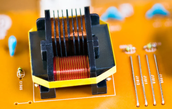
PCB transformer windings are typically implemented as spiral traces that may span multiple layers of the board:
- Single-layer spirals: Simple implementations where both primary and secondary are on the same layer
- Multi-layer spirals: Windings distributed across several layers to increase turns count
- Interleaved windings: Alternating primary and secondary turns to improve coupling and reduce leakage inductance
- Sandwich windings: Primary between two secondary layers or vice versa for better coupling
The geometric arrangement of these windings affects key parameters such as leakage inductance, parasitic capacitance, and current handling capability.
Design Considerations for PCB Transformers
Electrical Parameters
Designing an effective PCB transformer requires careful consideration of several electrical parameters:
- Turns Ratio: Determined by the required voltage transformation and implemented through the number of spiral turns in each winding.
- Current Density: PCB traces have limited current-carrying capacity compared to round wires, requiring careful calculation of trace width based on expected currents and acceptable temperature rise.
- Winding Resistance: The relatively thin copper layers in PCBs (typically 1 oz/ft² to 4 oz/ft²) result in higher DC resistance than conventional windings, impacting efficiency.
- Parasitic Elements: Inter-winding capacitance and leakage inductance are more pronounced in planar designs and must be carefully managed through proper spacing and winding geometry.
- Insulation Requirements: The PCB material must provide adequate dielectric strength between windings, especially for high-voltage applications.
Thermal Management
Effective thermal design is crucial for PCB transformers:
- Copper Weight: Thicker copper layers (2 oz/ft² or more) reduce resistive losses and improve heat dissipation.
- Thermal Vias: Arrays of vias can help transfer heat from inner layers to outer surfaces or dedicated heat sinking areas.
- Board Material: High-temperature substrates like polyimide or ceramic-filled materials can withstand greater thermal stress than standard FR-4.
- Layout Considerations: Adequate spacing between high-current traces and strategic placement of thermal relief patterns help manage temperature rise.
Manufacturing Considerations
PCB transformer designs must account for manufacturing capabilities and limitations:
- Trace Width/Spacing: Minimum feature sizes determined by PCB fabrication processes affect achievable winding density.
- Layer Count: More layers allow for more complex winding arrangements but increase cost.
- Via Reliability: High-current applications require robust via structures, possibly using filled or stacked vias.
- Registration Tolerance: Layer-to-layer alignment affects winding coupling and must be considered in the design.
- Testing Access: Incorporating test points for production testing without compromising performance.
Advantages of PCB Transformers
Size and Weight Reduction
The planar construction of PCB transformers offers significant advantages in terms of physical dimensions and weight:
- Low Profile: Typical heights of 5-10mm compared to 20-50mm for conventional transformers.
- Footprint Optimization: Can be designed to fit specific board areas rather than requiring dedicated mounting space.
- Weight Savings: Elimination of bulky bobbins and reduction in core material volume.
Improved Manufacturing Consistency
PCB fabrication processes provide excellent repeatability:
- Precision Windings: Trace geometries are photolithographically defined with micron-level precision.
- Automated Production: PCB manufacturing is highly automated, reducing variability between units.
- Scalability: Designs can be mass-produced without the labor-intensive winding processes of conventional transformers.
Enhanced Thermal Performance
The planar structure offers thermal advantages:
- Large Surface Area: Flat windings provide better heat dissipation to the PCB.
- Direct Heat Path: Thermal vias can efficiently conduct heat to heat sinks or other cooling structures.
- Uniform Temperature Distribution: Avoids hot spots common in wire-wound designs.
Integration Capabilities
PCB transformers enable higher levels of system integration:
- Embedded Components: Can be combined with other circuit elements on the same board.
- Modular Designs: Multiple transformers can be implemented on a single PCB for complex power conversion needs.
- Standardized Interfaces: Compatible with surface-mount assembly processes.
Applications of PCB Transformers
Power Electronics
PCB transformers are widely used in various power conversion applications:
- DC-DC Converters: Particularly in isolated topologies like flyback and forward converters.
- AC-DC Power Supplies: For line voltage isolation in compact power adapters.
- Inverters: In solar microinverters and other renewable energy systems.
Telecommunications
High-frequency signal isolation applications:
- LAN Transformers: For Ethernet interface isolation.
- xDSL Circuits: In digital subscriber line equipment.
- RF Isolation: In certain radio frequency applications.
Automotive Electronics
The automotive industry increasingly adopts PCB transformers:
- EV Power Systems: In onboard chargers and DC-DC converters for electric vehicles.
- LED Lighting Drivers: For automotive lighting systems.
- Battery Management: In voltage monitoring and isolation circuits.
Consumer Electronics
Compact power solutions for portable devices:
- USB Power Delivery: In high-power USB adapters.
- Wireless Charging: For resonant inductive power transfer systems.
- Audio Equipment: In professional audio isolation applications.
Industrial Electronics
Robust solutions for industrial environments:
- Process Control: For signal isolation in industrial automation.
- Motor Drives: In compact variable frequency drives.
- Measurement Equipment: Providing isolated measurement capabilities.
Challenges and Limitations
Despite their advantages, PCB transformers face several technical challenges:
Power Density Limitations
- Current Handling: Limited by copper thickness and trace width.
- Core Saturation: Planar cores may have lower saturation limits than conventional designs.
- Voltage Isolation: Achieving high-voltage isolation requires careful design of creepage and clearance.
High-Frequency Effects
- Skin Effect: High-frequency currents concentrate at trace surfaces, increasing effective resistance.
- Proximity Effect: Adjacent traces influence current distribution, further increasing losses.
- Parasitic Capacitance: Inter-winding capacitance can be significant at high frequencies.
Thermal Constraints
- Limited Cooling: Restricted airflow in compact designs challenges heat dissipation.
- Material Limitations: Standard PCB materials have relatively low thermal conductivity.
- Hot Spots: Uneven current distribution can create localized heating.
Manufacturing Constraints
- Layer Count: High-turn-ratio designs may require many layers, increasing cost.
- Copper Thickness: While thicker copper reduces resistance, it complicates etching processes.
- Yield Considerations: Complex designs with fine features may impact production yields.
Future Trends and Developments
Advanced Materials
Emerging materials promise improved performance:
- High-Temperature Substrates: Materials capable of withstanding higher operating temperatures.
- Nanocrystalline Cores: Offering superior magnetic properties for planar implementations.
- Embedded Magnetic Materials: Magnetic composites integrated directly into PCB substrates.
3D Integration
Novel manufacturing approaches:
- Multi-Chip Modules: Integrating transformers with other power components in 3D packages.
- Embedded Components: Transformers fully encapsulated within the PCB structure.
- Additive Manufacturing: 3D printing techniques for customized magnetic structures.
High-Frequency Designs
Pushing operational limits:
- MHz-Range Operation: For ultra-compact power converters.
- GaN and SiC Compatibility: Transformers optimized for wide-bandgap semiconductor switches.
- Resonant Converters: Designs optimized for LLC and other resonant topologies.
Smart Transformers
Integration of additional functionality:
- Integrated Sensors: Built-in temperature and current monitoring.
- Active Control Elements: Combining semiconductor devices with transformer structures.
- Self-Regulating Designs: Materials with temperature-dependent properties for automatic thermal management.
Conclusion
PCB transformers represent a transformative approach to electromagnetic component design, offering compelling advantages in size, manufacturability, and integration capability. While they present unique design challenges compared to conventional wire-wound transformers, ongoing advancements in materials, manufacturing techniques, and design methodologies continue to expand their application space.
As electronic systems trend toward higher power densities and greater integration, PCB transformers will play an increasingly vital role across industries from consumer electronics to electric vehicles and renewable energy systems. Future developments in magnetic materials, 3D integration, and high-frequency operation promise to further enhance their performance and broaden their applicability.
Engineers adopting PCB transformer technology must carefully balance electrical, thermal, and manufacturing considerations to fully realize their benefits. With proper design and implementation, PCB transformers offer a powerful solution for modern power electronics challenges, enabling the next generation of compact, efficient, and highly integrated electronic systems.