The Comprehensive Guide to BGA PCB Boards: Design, Manufacturing, and Applications
Introduction to BGA Technology
Ball Grid Array (BGA) printed circuit boards represent one of the most significant advancements in electronic packaging technology in recent decades. As electronic devices continue to shrink in size while increasing in functionality, BGA packages have become essential components in modern PCB design. This packaging solution addresses many of the limitations posed by traditional through-hole and surface-mount technologies, particularly for high-density integrated circuits.
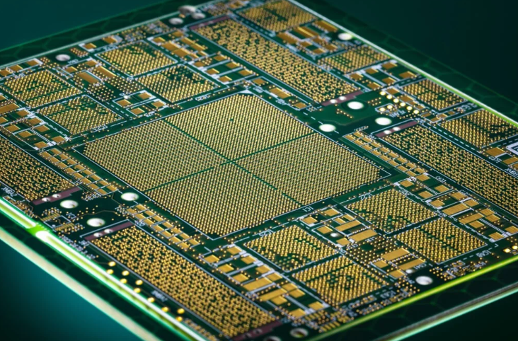
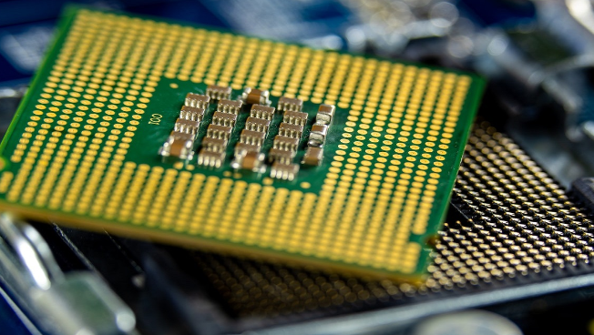
BGA technology replaces the peripheral leads found in conventional packages with an array of solder balls arranged in a grid pattern on the underside of the component. This fundamental architectural difference provides numerous advantages, including higher pin counts, improved thermal and electrical performance, and reduced footprint. Since its introduction in the 1990s, BGA packaging has evolved through several generations, with modern variants offering increasingly sophisticated solutions for today’s demanding electronic applications.
BGA Package Types and Variations
The BGA family encompasses several specialized package types, each designed to address specific requirements in electronic systems:
1. Standard BGA (PBGA): Plastic Ball Grid Array packages represent the most common BGA variant, featuring a plastic substrate and typically used for applications with moderate thermal requirements. PBGAs offer good electrical performance at relatively low cost, making them suitable for a wide range of consumer and industrial electronics.
2. Ceramic BGA (CBGA): Utilizing a ceramic substrate instead of plastic, CBGAs provide superior thermal conductivity and mechanical stability. These characteristics make them ideal for high-reliability applications in aerospace, military, and automotive electronics where extreme temperatures and harsh environments are common.
3. Tape BGA (TBGA): Featuring a flexible polyimide tape substrate, TBGAs offer an excellent balance between performance and cost. The thin profile of TBGA packages makes them particularly suitable for space-constrained applications like mobile devices.
4. Micro BGA (μBGA): As the name suggests, these packages represent a miniaturized version of standard BGAs, with ball pitches typically ranging from 0.3mm to 0.5mm. μBGAs enable extremely high-density interconnections for advanced microprocessors, FPGAs, and memory devices.
5. Chip-Scale BGA (CSBGA): These packages are only slightly larger than the silicon die itself (typically no more than 20% larger), representing the ultimate in miniaturization. CSBGAs are commonly found in smartphones, tablets, and wearable electronics where board space is at a premium.
6. Flip-Chip BGA (FCBGA): In this configuration, the silicon die is mounted upside-down (flipped) and connected directly to the substrate using solder bumps. FCBGAs offer superior electrical performance and thermal characteristics compared to wire-bonded alternatives, making them the package of choice for high-performance processors and ASICs.
BGA PCB Design Considerations
Designing PCBs for BGA components requires careful attention to numerous factors to ensure reliable operation and manufacturability:
1. Pad Design and Layout: BGA pads must be properly sized to match the solder balls while allowing for manufacturing tolerances. Non-solder mask defined (NSMD) pads are generally preferred as they provide better solder joint reliability. The pad diameter should typically be 80-90% of the ball diameter to ensure proper solder wetting and joint formation.
2. Escape Routing: One of the primary challenges in BGA design is routing signals from the dense array of balls to other board components. Several strategies exist for escape routing:
- Dog-bone fanout patterns for perimeter rows
- Via-in-pad technology for high-density designs
- Microvias and buried vias for complex multilayer boards
- Staggered via patterns to maximize routing channels
3. Via Selection: Via type and placement significantly impact BGA routing success. Through-hole vias work well for pitches down to 0.8mm, while microvias (laser-drilled) are essential for finer pitches. Blind and buried vias can help optimize routing density in complex designs.
4. Thermal Management: BGAs, especially high-power devices, require careful thermal design:
- Thermal vias under exposed pads to conduct heat to inner layers
- Copper pours and thermal relief patterns
- Consideration of thermal interface materials for high-power devices
- Potential need for heatsinks or active cooling solutions
5. Signal Integrity: High-speed BGA devices demand attention to:
- Controlled impedance routing
- Length matching for differential pairs
- Proper power delivery network design
- Minimizing via stubs for high-frequency signals
BGA Assembly Processes
The assembly of BGA components onto PCBs involves specialized processes that differ significantly from conventional SMT assembly:
1. Solder Paste Printing: Precise solder paste deposition is critical for BGA assembly. Stencil design must account for:
- Appropriate aperture size and shape (typically circular or square)
- Stencil thickness (usually 0.1mm to 0.15mm for standard BGAs)
- Nano-coated stencils for improved paste release
2. Component Placement: BGA placement requires high-accuracy pick-and-place machines capable of:
- Vision alignment using fiducials and package features
- Precise force control to prevent damage to solder balls
- Placement accuracy within ±25μm for fine-pitch BGAs
3. Reflow Soldering: The reflow profile is crucial for proper BGA joint formation:
- Typical peak temperatures of 235-245°C for SAC305 solder
- Careful control of time above liquidus (typically 60-90 seconds)
- Nitrogen atmosphere may be used to improve wetting
- Thermal profiling to ensure even heating across large packages
4. Inspection and Testing: BGA joints present unique inspection challenges:
- X-ray inspection is essential for hidden solder joints
- Automated optical inspection (AOI) for visible alignment
- Boundary scan testing for electrical verification
- Acoustic microscopy for void detection
5. Rework Processes: BGA rework requires specialized equipment:
- Precision hot air systems with bottom heating
- Thermocouple monitoring for temperature control
- Vacuum pickup tools for component handling
- Solder paste or preforms for joint reformation
Advantages of BGA Technology
The widespread adoption of BGA packaging across virtually all segments of the electronics industry stems from numerous compelling advantages:
1. High Interconnection Density: BGA packages can accommodate hundreds or even thousands of interconnections in a relatively small footprint. The array configuration allows for efficient use of space beneath the component, unlike perimeter-leaded packages where pin count increases directly with package size.
2. Improved Electrical Performance: The shorter interconnection paths in BGA packages result in:
- Reduced inductance (typically 0.1-0.5nH vs. 2-5nH for QFPs)
- Lower capacitance between leads
- Better high-frequency characteristics
- Improved signal integrity for high-speed interfaces
3. Enhanced Thermal Characteristics: BGA packages generally offer superior thermal performance compared to leaded packages:
- Direct thermal path through solder balls to the PCB
- Ability to incorporate large thermal pads
- Option for thermal vias under the package
- More efficient heat spreading through the substrate
4. Manufacturing Benefits: BGA technology provides several production advantages:
- Self-alignment during reflow due to surface tension
- Reduced sensitivity to placement accuracy compared to fine-pitch QFPs
- Higher assembly yields for high-pin-count devices
- Better resistance to mechanical stress during handling
5. Reliability Improvements: Properly designed BGA assemblies demonstrate:
- Better resistance to mechanical shock and vibration
- Reduced sensitivity to thermal cycling stresses
- Lower susceptibility to coplanarity issues
- Improved long-term connection reliability
Challenges and Limitations
Despite their many advantages, BGA packages present several challenges that designers and manufacturers must address:
1. Inspection Difficulties: The hidden nature of BGA solder joints makes visual inspection impossible, requiring expensive X-ray equipment for proper quality control. This limitation complicates failure analysis and process verification.
2. Rework Complexity: Removing and replacing BGA components demands specialized equipment and skilled operators. The process is more time-consuming and costly compared to reworking conventional SMT components.
3. PCB Complexity Requirements: High-density BGA components often necessitate:
- High-layer-count PCBs (8+ layers common)
- Advanced PCB technologies like HDI and microvias
- Tight manufacturing tolerances
- Expensive substrate materials for high-speed designs
4. Thermal Stress Considerations: The CTE (Coefficient of Thermal Expansion) mismatch between components and PCB can lead to:
- Solder joint fatigue during thermal cycling
- Warpage issues during assembly
- Reliability concerns in extreme environments
5. Cost Factors: While BGA technology offers many benefits, it also introduces additional costs:
- Higher PCB fabrication expenses
- Specialized assembly equipment requirements
- Increased testing and inspection costs
- Higher initial tooling investments
Applications of BGA PCB Technology
BGA packages have found widespread adoption across virtually all segments of the electronics industry:
1. Computing Systems:
- CPUs and GPUs in desktops, laptops, and servers
- Chipset components on motherboards
- High-performance memory modules
- Solid-state drive controllers
2. Telecommunications:
- Network processors in routers and switches
- Baseband processors in cellular infrastructure
- High-speed SerDes devices
- Optical networking components
3. Consumer Electronics:
- Application processors in smartphones and tablets
- Multimedia SoCs in TVs and set-top boxes
- Gaming console main processors
- Wearable device controllers
4. Automotive Electronics:
- Advanced driver assistance systems (ADAS)
- Infotainment system processors
- Engine control units
- Autonomous vehicle computing platforms
5. Industrial and Medical:
- Industrial automation controllers
- Medical imaging equipment
- Test and measurement instruments
- Robotics control systems
Future Trends in BGA Technology
As electronic systems continue to evolve, BGA packaging is advancing to meet emerging requirements:
1. Finer Pitches: The ongoing trend toward smaller ball pitches (approaching 0.2mm) enables even higher interconnection densities while presenting new manufacturing challenges.
2. 3D Packaging: Stacked die configurations and package-on-package (PoP) arrangements leverage BGA technology for vertical integration, particularly in mobile applications.
3. Advanced Materials: New substrate materials with improved thermal and electrical properties are being developed to support higher-performance devices.
4. Heterogeneous Integration: BGA packages are increasingly incorporating multiple die types (logic, memory, RF) in single packages for system-level solutions.
5. Thermal Solutions: Innovative cooling approaches, including embedded heat spreaders and vapor chambers, are being integrated into BGA packages for high-power applications.
Conclusion
BGA PCB technology has become indispensable in modern electronics, offering an optimal balance between performance, density, and manufacturability. While presenting certain design and production challenges, the benefits of BGA packaging far outweigh its limitations for a vast range of applications. As electronic systems continue their relentless march toward higher performance and miniaturization, BGA technology will undoubtedly evolve to meet these demands, maintaining its position as a cornerstone of electronic packaging for years to come.
Understanding BGA PCB design, manufacturing processes, and application considerations is essential for electronics engineers, PCB designers, and manufacturing professionals working with contemporary electronic systems. By mastering BGA technology, professionals can develop more advanced, reliable, and cost-effective electronic products that meet the ever-increasing demands of the marketplace.