Ceramic RF PCBs: Design, Materials, and Applications in High-Frequency Electronics
Introduction to Ceramic RF PCBs
Radio Frequency (RF) printed circuit boards (PCBs) represent a specialized category of circuit boards designed to operate at high frequencies, typically ranging from a few megahertz (MHz) to several gigahertz (GHz) and beyond. Among the various substrate materials available for RF applications, ceramic-based PCBs have emerged as a superior solution for demanding high-frequency applications due to their exceptional electrical, thermal, and mechanical properties.
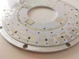
Ceramic RF PCBs utilize ceramic materials as their substrate instead of the more common FR-4 or other organic laminates. These advanced circuit boards have become indispensable in modern wireless communication systems, aerospace and defense electronics, automotive radar systems, and medical imaging equipment where high-frequency performance, thermal management, and reliability are critical.
Ceramic Materials for RF PCB Substrates
Common Ceramic Substrate Materials
Several ceramic materials have proven particularly suitable for RF PCB applications:
- Alumina (Al₂O₃): The most widely used ceramic substrate, available in various purity levels (96% to 99.5%). Offers good thermal conductivity (20-30 W/mK) and excellent electrical insulation.
- Aluminum Nitride (AlN): Features exceptional thermal conductivity (140-180 W/mK) while maintaining good electrical insulation. Ideal for high-power RF applications.
- Beryllium Oxide (BeO): Provides the highest thermal conductivity among ceramics (250-300 W/mK) but poses health hazards during machining due to toxic dust.
- Low-Temperature Co-fired Ceramic (LTCC): A glass-ceramic composite that can be fired at relatively low temperatures (850-900°C), allowing for the integration of conductive materials with lower melting points.
- High-Temperature Co-fired Ceramic (HTCC): Uses pure ceramic materials fired at high temperatures (1600-1800°C), offering superior performance but requiring refractory metals for conductors.
Key Properties of Ceramic Substrates
Ceramic materials offer several advantages for RF applications:
- Low Dielectric Loss (tan δ): Minimizes signal attenuation at high frequencies
- Stable Dielectric Constant (εᵣ): Provides consistent performance across temperature variations
- Excellent Thermal Conductivity: Efficient heat dissipation from active components
- Low Thermal Expansion Coefficient (CTE): Matches well with semiconductor devices, reducing thermal stress
- High Mechanical Strength: Maintains structural integrity in harsh environments
- Hermetic Properties: Naturally resistant to moisture absorption and gas permeation
Design Considerations for Ceramic RF PCBs
Transmission Line Structures
Proper transmission line design is crucial for maintaining signal integrity in RF circuits:
- Microstrip Lines: A conductor on the top layer with a ground plane beneath, separated by the ceramic dielectric. Commonly used for its simplicity and ease of integration with surface-mount components.
- Stripline: A conductor sandwiched between two ground planes within the ceramic substrate. Offers better shielding but is more complex to manufacture.
- Coplanar Waveguide (CPW): Consists of a center conductor with ground planes on the same layer. Provides excellent high-frequency performance and easier integration with shunt components.
- Ground Coplanar Waveguide (GCPW): Combines features of microstrip and CPW, with additional ground planes on both sides of the signal line.
Impedance Matching
Maintaining consistent characteristic impedance throughout the RF circuit is essential to minimize reflections:
- Typical impedance values: 50Ω for most RF systems, 75Ω for video applications
- Impedance calculation depends on the transmission line geometry, conductor dimensions, and ceramic dielectric constant
- Tapered transitions are often necessary when connecting different transmission line types
Via Design
Proper via implementation is critical in ceramic RF PCBs:
- Blind and Buried Vias: Used to create complex interconnections while minimizing stub effects
- Via Filling: Often employed with conductive materials to improve thermal and electrical performance
- Via Fencing: Creates effective shielding for sensitive RF components
- Via Aspect Ratio: More manageable in ceramic substrates compared to organic PCBs due to ceramic’s mechanical strength
Manufacturing Processes for Ceramic RF PCBs
Thin-Film Technology
Thin-film ceramic PCBs offer the highest precision for RF applications:
- Substrate Preparation: Ceramic substrates are polished to achieve ultra-smooth surfaces
- Metal Deposition: Sputtering or evaporation of adhesion layers (Ti, Cr) followed by conductor layers (Au, Cu)
- Patterning: Photolithography followed by etching to create precise circuit patterns
- Post-Processing: Additional plating or surface treatments as needed
Thick-Film Technology
A more cost-effective approach suitable for many RF applications:
- Screen Printing: Conductive, resistive, and dielectric pastes are deposited through patterned screens
- Drying and Firing: Each layer is dried and fired at high temperatures to achieve adhesion and desired properties
- Multilayer Construction: Multiple printing/firing cycles build up complex circuits
LTCC/HTCC Technology
Co-fired ceramic technologies enable highly integrated RF modules:
- Green Tape Processing: Ceramic in unfired (“green”) state is processed with conductor printing
- Lamination: Multiple layers are aligned and laminated under pressure
- Co-firing: The entire stack is fired in a controlled atmosphere furnace
- Post-Fire Processing: Additional components or features may be added after firing
Applications of Ceramic RF PCBs
Aerospace and Defense Systems
- Radar systems (phased array antennas, tracking radars)
- Electronic warfare systems (jammers, countermeasure systems)
- Satellite communication subsystems
- Missile guidance systems
Telecommunications Infrastructure
- 5G base stations and small cells
- Millimeter-wave communication systems
- RF power amplifiers and filters
- Antenna arrays and beamforming networks
Automotive Electronics
- Automotive radar systems (77GHz for ADAS)
- Vehicle-to-everything (V2X) communication modules
- High-frequency sensors for autonomous vehicles
Medical Electronics
- MRI systems
- RF ablation equipment
- Medical imaging systems
- Wireless implantable devices
Test and Measurement Equipment
- Spectrum analyzers
- Network analyzers
- High-frequency signal generators
- RF probe cards for semiconductor testing
Advantages of Ceramic RF PCBs Over Conventional PCBs
Electrical Performance Benefits
- Lower dielectric loss (tan δ) at high frequencies
- More stable dielectric constant (εᵣ) with frequency and temperature
- Better controlled impedance characteristics
- Reduced parasitic effects due to thinner substrates
Thermal Management Advantages
- Superior thermal conductivity (5-20 times better than FR-4)
- Better CTE matching with semiconductor devices
- Ability to handle high power densities
- Reliable operation at elevated temperatures
Reliability and Environmental Stability
- Hermetic properties prevent moisture absorption
- Resistant to chemical corrosion
- Excellent mechanical stability under thermal cycling
- Long-term reliability in harsh environments
Challenges and Limitations of Ceramic RF PCBs
Cost Considerations
- Raw material costs significantly higher than organic substrates
- Specialized manufacturing equipment required
- Lower production volumes compared to conventional PCBs
- More complex design and testing requirements
Manufacturing Challenges
- Brittle nature requires careful handling
- Limited substrate sizes available
- Difficult to modify or rework after production
- Specialized equipment needed for processing
Design Limitations
- Higher dielectric constant may lead to larger wavelengths
- Limited layer count compared to multilayer organic PCBs
- Challenges in integrating with conventional PCB assemblies
- Special considerations needed for component attachment
Future Trends in Ceramic RF PCB Technology
Advanced Materials Development
- Nanocomposite ceramics with tailored properties
- Glass-ceramic hybrids for improved processability
- Low-loss dielectric materials for mmWave applications
- Graphene-enhanced ceramic substrates
Integration Technologies
- Embedded active and passive components
- 3D packaging approaches
- Heterogeneous integration with organic substrates
- System-in-package (SiP) solutions
Manufacturing Innovations
- Additive manufacturing of ceramic circuits
- Laser-based processing techniques
- Automated optical inspection for high-density circuits
- Advanced metrology for quality control
Emerging Application Areas
- 6G communication systems
- Quantum computing interfaces
- Terahertz imaging systems
- Space-based internet constellations
Conclusion
Ceramic RF PCBs represent a critical enabling technology for modern high-frequency electronic systems. Their unique combination of excellent high-frequency performance, superior thermal management, and exceptional reliability makes them indispensable in demanding applications ranging from 5G telecommunications to aerospace radar systems. While challenges remain in terms of cost and manufacturability, ongoing advancements in ceramic materials, design methodologies, and processing technologies continue to expand the capabilities and applications of these specialized circuit boards.
As wireless technologies push into higher frequency ranges and systems require increasing levels of integration and performance, ceramic RF PCBs will play an increasingly vital role in enabling these next-generation electronic systems. Engineers and designers working in RF and microwave fields must understand both the capabilities and limitations of ceramic PCB technologies to fully leverage their advantages in cutting-edge electronic designs.
The future of ceramic RF PCBs looks promising, with new materials and manufacturing techniques poised to address current limitations while opening up novel applications in emerging technological fields. As the demand for high-frequency, high-reliability electronic systems continues to grow across multiple industries, ceramic-based solutions will remain at the forefront of RF PCB technology.