PCB Sharp Angles: Design Tips for Modern Manufacturing

Key Takeaways
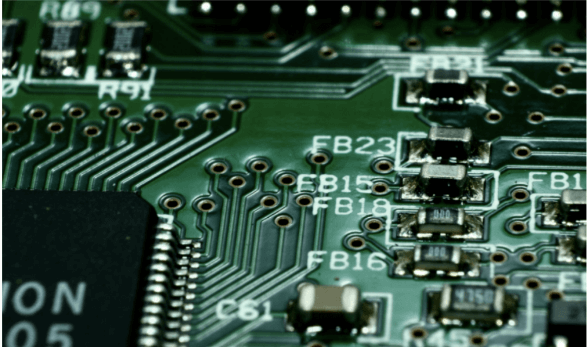
When designing PCBs with sharp angles, understanding PCB manufacturing constraints becomes critical. Modern PCB manufacturing companies often recommend avoiding 90-degree traces due to potential signal integrity issues and etching challenges. Instead, opt for 45-degree angles or curved traces to minimize current crowding and improve reliability.
Tip: Always verify your design with PCB manufacturing cost considerations in mind—small adjustments to trace widths or via sizes can reduce material waste and lower production expenses.
If sharp angles are unavoidable, ensure trace widths remain consistent to prevent impedance mismatches. For vias near angled traces, follow via size selection best practices (e.g., larger vias for high-current paths) to avoid thermal stress. When using tools like KiCad, leverage built-in routing features to automate angle adjustments while maintaining design intent.
Balancing aesthetic preferences with PCB manufacturing business realities requires collaboration with your fabrication partner. Discuss manufacturing tolerances early—most facilities can handle angles down to 30 degrees, but tighter tolerances may increase costs. By prioritizing manufacturability, you’ll achieve designs that perform reliably without compromising scalability.
Sharp Angles in Modern PCB Production
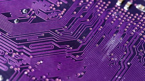
When designing circuit boards, you might encounter situations where sharp angles seem unavoidable. However, modern PCB manufacturing processes demand careful consideration of these geometries. While 90-degree angles were once common, today’s high-frequency applications and miniaturized components require smoother transitions to prevent signal reflection and electromagnetic interference. Most PCB manufacturing companies now recommend using 45-degree angles or curved traces, as sharp corners can create acid traps during etching, leading to uneven copper removal and potential short circuits.
To balance performance and PCB manufacturing cost, consider these factors:
| Design Feature | Risk with Sharp Angles | Mitigation Strategy |
|---|---|---|
| Trace junctions | Increased impedance discontinuity | Use chamfered or rounded corners |
| High-speed signal paths | Signal integrity degradation | Maintain consistent trace widths |
| Thermal management | Localized heat accumulation | Optimize pad shapes and spacing |
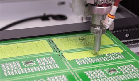
Advanced fabrication tools allow tighter tolerances, but design choices still directly impact yield rates and PCB manufacturing business margins. For instance, collaborating closely with your manufacturer helps identify angle-related constraints early, avoiding costly re-spins. Remember: what looks acceptable in simulation might not survive physical production—prioritize manufacturability alongside electrical performance.
Optimizing Trace Widths for Reliability
When designing traces with sharp angles, balancing electrical performance and manufacturability starts with selecting appropriate trace widths. Narrow traces may reduce PCB manufacturing cost by conserving copper, but they risk overheating or breaking under high current. Conversely, overly wide traces complicate routing in dense layouts, potentially increasing PCB manufacturing business expenses due to material waste or design revisions.
To ensure reliability, calculate your trace width based on current load, thermal dissipation, and the fabrication tolerances of your chosen PCB manufacturing companies. For example, a 10-mil trace might handle 1A in standard FR-4 boards, but sharp angles can create localized current crowding, necessitating slight width adjustments. Tools like KiCad’s built-in calculators simplify this process by factoring in material properties and temperature rise.
Remember that PCB manufacturing processes vary—subtle differences in etching precision between suppliers might affect minimum achievable widths. Always verify your design against the manufacturer’s technical guidelines to avoid unexpected impedance mismatches or signal integrity issues. By optimizing trace widths early, you reduce the risk of costly rework while maintaining compatibility with modern PCB manufacturing standards.
This balance becomes critical when transitioning between angled and straight segments, as abrupt changes in width can trap acids during etching—a topic explored further in the next section.
Via Size Selection Best Practices
When selecting via sizes for your PCB design, balance electrical requirements with pcb manufacturing realities. Start by understanding your fabricator’s capabilities—most pcb manufacturing companies specify minimum via diameters (typically 0.15–0.3mm) and aspect ratios (drill depth to diameter) below 8:1. Oversizing vias reduces impedance and improves current handling but increases pcb manufacturing cost by requiring more material and processing time. Conversely, undersized vias risk drill breakage or incomplete plating, leading to reliability failures.
For signal vias, prioritize a diameter-to-pad ratio that accommodates annular ring requirements (≥0.05mm). Power and ground vias often demand larger sizes (≥0.4mm) to handle higher currents. Use stacked or staggered microvias in high-density designs, but confirm your pcb manufacturing business partner supports advanced laser drilling. Always cross-verify thermal relief settings to prevent uneven copper distribution during plating.
Transitioning from trace width optimization, remember that via placement affects routing efficiency. Align via grids with component footprints in KiCad to minimize acid trap risks while maintaining signal integrity. By aligning your via strategy with both design goals and pcb manufacturing tolerances, you avoid costly revisions and ensure production scalability.
KiCad Routing Techniques for Beginners
When starting with PCB manufacturing design in KiCad, mastering routing fundamentals ensures your board meets both functional and production requirements. Begin by using the Interactive Router tool, which allows you to define trace paths while avoiding sharp angles automatically. Set your grid spacing to match your PCB manufacturing companies’ preferred tolerances—this minimizes manual adjustments and ensures cleaner routing.
For complex layouts, prioritize shorter traces between components to reduce signal interference. Use 45-degree angles instead of 90-degree turns wherever possible, as sharp corners can trap acid during etching, increasing PCB manufacturing cost due to rework. KiCad’s Differential Pair Routing feature helps maintain consistent spacing for high-speed signals, critical for modern designs.
Another key consideration is layer stacking: align your routing strategy with the fabrication capabilities of your chosen PCB manufacturing business. For example, if they specialize in low-cost, two-layer boards, avoid overcomplicating via placements. Use the Design Rule Checker (DRC) to flag potential issues like insufficient clearances or acute angles before finalizing files.
Finally, practice modular routing—group related traces and components to simplify troubleshooting. This approach not only streamlines your workflow but also aligns with industry standards, ensuring your design transitions smoothly from KiCad to production.
Avoiding Acid Traps in PCB Design
When designing traces with angles, you must consider how PCB manufacturing processes handle chemical etching. Sharp corners (below 90 degrees) create acid traps—areas where etching fluid pools and erodes copper unevenly, risking open circuits or unintended shorts. To prevent this, prioritize curved traces or 45-degree angles, which allow chemicals to flow freely during production.
Many PCB manufacturing companies recommend maintaining a minimum internal angle of 90 degrees for critical signal paths. This reduces the likelihood of residual acid compromising trace integrity. If sharp angles are unavoidable—for example, in high-density layouts—collaborate with your fabricator early to adjust trace-to-space ratios or apply teardrop shapes at junctions. Such adjustments might marginally increase PCB manufacturing cost, but they significantly improve yield rates and long-term reliability.
For designs targeting cost-sensitive applications, like consumer electronics, balancing aesthetic preferences with fabrication realities becomes crucial. Overly aggressive angles might look appealing but often lead to rework in the PCB manufacturing business. Use design rule checks (DRCs) in tools like KiCad to flag potential acid traps automatically, and always cross-verify with your manufacturer’s capabilities before finalizing layouts.
Manufacturing Tolerances for PCB Angles
When designing PCBs with sharp angles, understanding manufacturing tolerances is critical to avoid unexpected production challenges. PCB manufacturing processes rely on precise etching and drilling, but even advanced PCB manufacturing companies face limitations when handling acute angles below 30 degrees. These tight geometries can lead to copper thinning or incomplete etching, particularly if your design pushes the limits of standard fabrication equipment.
Most manufacturers specify a minimum angle tolerance of 45 degrees for reliable results, though high-end facilities may achieve tighter tolerances at increased PCB manufacturing cost. Always verify your fabricator’s capabilities early in the design phase—this ensures your angled traces or custom via patterns align with their equipment’s resolution. For example, smaller PCB manufacturing business operations might use older machinery, limiting their ability to maintain consistency in designs with extreme angles.
To balance performance and manufacturability, prioritize angle rounding in high-current traces or RF circuits where sharp corners risk signal integrity. Transitioning to curved or chamfered angles not only reduces fabrication risks but also aligns with modern PCB manufacturing standards. Remember: tighter tolerances often mean higher costs, so weigh aesthetic preferences against functional and budgetary constraints when finalizing your design.
PCB Angle Design Guidelines 2024
When designing angled traces in 2024, you must balance geometric precision with PCB manufacturing realities. Modern PCB manufacturing companies prioritize designs that minimize acute angles (below 90°) to reduce risks like signal reflection and copper cracking. Start by aligning trace bends with PCB manufacturing cost constraints—using 45° or curved transitions instead of sharp corners improves yield rates while maintaining signal integrity.
For high-density boards, adhere to 0.3mm minimum radius recommendations for curved traces, as tighter bends increase PCB manufacturing business challenges like copper lift-off. Pair this with adaptive trace widths—thinner traces (≤0.2mm) near angles require gradual tapering to avoid impedance mismatches. Advanced tools like automated DRC checks in KiCad now flag problematic angles, but always validate designs against your fabricator’s tolerance thresholds (typically ±10% for angle precision).
Aim for uniform via placement near angled junctions, as clustered vias strain PCB manufacturing processes. For example, pairing 0.15mm drill sizes with 0.25mm annular rings ensures reliability without inflating costs. Finally, integrate acid trap prevention into your workflow by avoiding narrow solder mask gaps around sharp features—this reduces rework and aligns with 2024’s focus on first-pass success in fabrication.
Balancing Aesthetics and Functionality
When designing PCBs, you’re often torn between creating visually clean layouts and meeting strict technical requirements. Sharp angles might look sleek in your CAD software, but PCB manufacturing processes prioritize functionality over form. For instance, 90-degree corners can cause signal reflections or uneven copper etching, leading to reliability issues. Modern PCB manufacturing companies often recommend curved or 45-degree traces to minimize these risks while maintaining a balanced aesthetic.
To align aesthetics with performance, consider how PCB manufacturing cost factors into your design choices. Overly complex angles may require specialized tooling or additional fabrication steps, increasing expenses. Instead, focus on optimizing trace widths and via sizes—critical parameters that influence both electrical performance and visual coherence. Tools like KiCad’s interactive router help automate this balance, allowing you to prioritize signal integrity without sacrificing design elegance.
Remember, PCB manufacturing business standards emphasize designs that are both functional and reproducible. Avoid over-engineering artistic features that complicate assembly or testing. For example, tightly packed traces with sharp angles might look impressive but could violate clearance rules or create acid traps during etching. By collaborating early with fabrication partners, you can refine your designs to meet technical tolerances while preserving a polished appearance—ensuring your boards perform reliably and look professional.
Conclusion
In modern PCB design, balancing sharp angles with manufacturing feasibility requires deliberate planning. By integrating optimized trace widths and via sizing with your pcb manufacturing partner’s capabilities, you minimize risks like signal interference or fabrication errors. While pcb manufacturing companies can handle complex geometries, pushing tolerances too far increases pcb manufacturing cost and delays. Stick to industry-standard angle guidelines unless specific applications demand tighter controls—this ensures compatibility across fabrication processes. For those managing a pcb manufacturing business, prioritizing designs that align with common tooling setups reduces overhead while maintaining quality. Remember: even minor adjustments in KiCad routing or acid trap prevention create cumulative efficiency gains. Always validate your design choices against your manufacturer’s technical specs to avoid costly revisions.
FAQs
How do sharp angles affect signal integrity in high-frequency designs?
Sharp angles can create impedance mismatches and reflections, particularly in RF circuits. Most PCB manufacturing companies recommend using 45° or curved traces for high-speed signals to maintain consistent impedance and reduce electromagnetic interference.
What’s the relationship between trace width and PCB manufacturing cost?
Narrower traces require tighter tolerances, increasing fabrication complexity. While modern PCB manufacturing processes can handle 3-4 mil traces, pushing limits may raise costs by 15-25% due to additional quality checks and potential yield losses.
Can KiCad’s autorouter handle sharp angles effectively?
KiCad’s autorouter prioritizes 45° angles by default, but manual adjustments are often needed for complex layouts. Always verify clearance rules with your PCB manufacturing business partner to avoid acid traps or etching issues.
Why do manufacturing tolerances matter for angled traces?
Tolerances determine how precisely fabricators can reproduce your design. For angles below 30°, discuss capability limits with your PCB manufacturing provider—some may require design rule adjustments to maintain reliability.
How do you balance aesthetics with functionality in angular designs?
While sharp angles might look sleek, prioritize electrical performance. Use angles judiciously in non-critical sections and adhere to your PCB manufacturing company’s design-for-manufacturing (DFM) guidelines to avoid compromising reliability.
Ready to Optimize Your PCB Design?
For tailored solutions that align with modern PCB manufacturing standards, please click here to consult our engineering team.


