Several details of PCB board layout
The layout of components in PCB board is crucial. Correct and reasonable layout not only makes the layout more neat and beautiful, but also affects the length and number of printed wires. Good PCB device layout is extremely important to improve the performance of the whole machine.
So how to make the layout more reasonable? Today we will share with you “Several details of PCB board layout”.
1.Key points of pc layout with wireless module
Analog circuits and digital circuits are physically separated, for example, the antenna ports of MCU and wireless module are as far away as possible;
Try to avoid arranging high-frequency digital routing, high-frequency analog routing, power routing and other sensitive devices under the wireless module, and copper can be laid under the module;
The wireless module should be kept as far away as possible from parts with large electromagnetic interference such as transformers, high-power inductors, and power supplies;
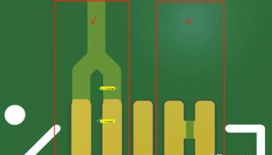
When placing a board-mounted PCB antenna or ceramic antenna, the PCB under the antenna part of the module needs to be hollowed out, copper should not be laid, and the antenna part should be as close to the board as possible;
Whether the RF signal or other signal routing should be as short as possible, other signals should also be away from the wireless module transmitter part to avoid interference;
Layout needs to consider that the wireless module needs to have a relatively complete power ground, and the RF routing needs to leave space for the ground hole;
The voltage ripple required by the wireless module is relatively high, so it is best to add a more appropriate filter capacitor close to the module voltage pin, such as 10uF;
The wireless module has a fast transmission frequency and has certain requirements for the transient response of the power supply. In addition to selecting a power supply solution with excellent performance during design, it is also necessary to pay attention to the reasonable layout of the power supply circuit during layout to give full play to the power supply performance; such as DC-DC layout, it is necessary to pay attention to the distance between the freewheeling diode ground and the IC ground as close as possible to ensure reflux, and the distance between the power inductor and the capacitor as close as possible.
2.Setting of line width and line spacing
The setting of line width and line spacing has a huge impact on the performance improvement of the entire board. Reasonable setting of line width and line spacing can effectively improve the electromagnetic compatibility and various aspects of performance of the entire board.
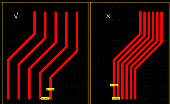
For example, the width of the power line should be set based on the current of the whole machine load, the power supply voltage, the copper thickness of the PCB, the length of the line, etc. Usually, a line with a width of 1.0mm and a copper thickness of 1oz (0.035mm) can pass a current of about 2A. Reasonable setting of the line spacing can effectively reduce crosstalk and other phenomena, such as the commonly used 3W principle (that is, when the center spacing between the wires is not less than 3 times the line width, 70% of the electric field can be kept from interfering with each other).
Power line routing: According to the current, voltage size and PCB copper thickness of the load, the current usually needs to be reserved twice the normal working current, and the line spacing should meet the 3W principle as much as possible.
Signal routing: According to the comprehensive consideration of the signal transmission rate, transmission type (analog or digital), routing length, etc., the spacing of ordinary signal lines is recommended to meet the 3W principle, and differential lines are considered separately.
RF routing: The line width of the RF routing needs to consider the characteristic impedance. The commonly used RF module antenna interface is 50Ω characteristic impedance. According to experience, the RF line width of ≤30dBm (1W) is 0.55mm, and the copper spacing is 0.5mm. More accurate characteristic impedance of about 50Ω can also be obtained through adjustment with the assistance of the board factory.
3.Setting the spacing between devices
During PCB layout, the spacing between devices is something we must consider. If the spacing is too small, it is easy to cause soldering and affect production;
The distance recommendations are as follows:
Similar devices: ≥0.3mm
Different devices: ≥0.13*h+0.3mm (h is the maximum height difference of the surrounding adjacent devices)
The distance between devices that can only be manually soldered is recommended: ≥1.5mm
DIP devices and SMD devices should also maintain a sufficient distance in production, and it is recommended to be between 1-3mm;
4.Control of the spacing between the board edge and the device and trace
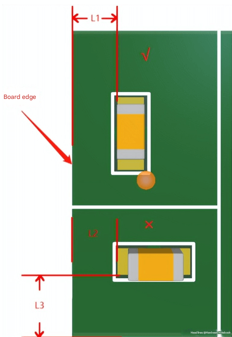
Whether the distance design between the device and the trace from the board edge is reasonable during PCB layout and routing is also very important. For example, in the actual production process, most of the panels are assembled. Therefore, if the device is too close to the board edge, it will cause the pad to fall off when the PCB is divided, or even damage the device. If the line is too close, it is easy to cause the line to break during production and affect the circuit function.
Recommended distance and placement:
Device placement: It is recommended that the device pads be parallel to the “V cut” direction of the panel, so that the mechanical stress on the device pads is uniform and the force direction is the same when the panel is separated, reducing the possibility of pads falling off.
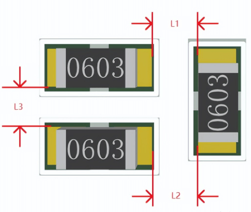
Device distance: The placement distance of the device from the edge of the board is ≥0.5mm
Trace distance: The distance between the trace and the edge of the board is ≥0.5mm
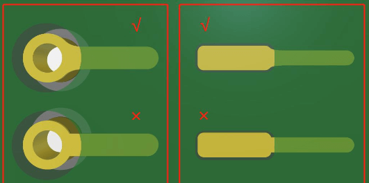
5.Adjacent pad connection and teardrop
If the adjacent pins of the IC need to be connected, it should be noted that it is best not to connect directly on the pads, but to lead out the connection outside the pads, so as to prevent the IC pins from being short-circuited during production. In addition, the line width between adjacent pads should also be noted, and it is best not to exceed the size of the IC pins, except for some special pins such as power pins.
Teardrops can effectively reduce the reflection caused by sudden changes in line width, and can make the traces and pads connect smoothly;
Adding teardrops solves the problem that the connection between the trace and the pad is easily broken by impact;
From the appearance point of view, adding teardrops can also make the PCB look more reasonable and beautiful;
6.Parameters and placement of vias
The reasonableness of the via size setting has a great impact on the performance of the circuit. Reasonable via size setting needs to consider the current, signal frequency, manufacturing process difficulty, etc. that the via bears, so PCB Layout needs special attention.
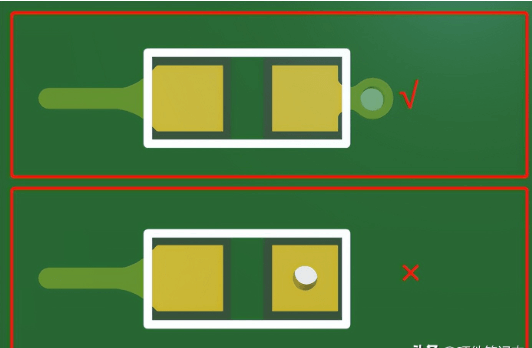
In addition, the placement of the via is also important. If the via is placed on the pad, it is easy to cause poor device welding during production. Therefore, the via is generally placed outside the pad. Of course, in the case of extremely tight space, the via is placed on the pad and the board manufacturer’s plate-in-hole process is also possible, but this will increase the production cost.
Key points of via setting:
Different sizes of vias can be placed in a PCB due to the needs of different routings, but it is usually not recommended to exceed 3 types to avoid causing great inconvenience to production and raising costs;
The depth to diameter ratio of the via is generally ≤6, because when it exceeds 6 times, it is difficult to ensure that the hole wall can be evenly copper plated;
The parasitic inductance and parasitic capacitance of the via also need to be paid attention to, especially in high-speed circuits, special attention should be paid to its distributed performance parameters;
The smaller the via, the smaller the distributed parameters, the more suitable it is for high-speed circuits, but its cost is also high;
The above 6 points are some precautions for PCB Layout sorted out this time, I hope it can be helpful to everyone.