Agile PCB Prototype Assembly for Next-Gen Innovations
Key Takeaways
Modern PCB assembly (PCBA) processes have become foundational to accelerating innovation in fields like IoT, AI, and robotics. By leveraging agile manufacturing frameworks, engineers can iterate designs rapidly while maintaining precision and cost efficiency. Below are critical insights for optimizing prototype development:
| Service Feature | Key Benefit | Ideal Application |
|---|---|---|
| Rapid Prototyping | Reduces time-to-market by 30-50% | IoT sensor integration |
| Flexible Batch Sizes | Supports small-scale R&D validation | AI hardware testing |
| Multi-Layer PCB Support | Enhances circuit density and performance | Robotics control systems |
"Agile PCBA methodologies enable engineers to validate concepts faster, bridging the gap between theoretical designs and functional prototypes." – Industry Expert
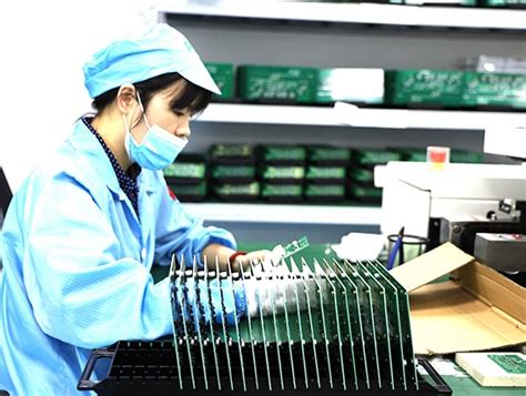
For teams developing next-gen technologies, prioritizing PCB assembly partners with expertise in high-frequency materials and thermal management is crucial. A streamlined workflow often integrates automated optical inspection (AOI) to ensure reliability, particularly for mission-critical prototypes.
Tip: When selecting a PCBA provider, verify their capability to handle mixed-technology boards (SMT + through-hole) and adherence to IPC-A-610 standards. This ensures compatibility with both low-power IoT devices and high-performance robotics architectures. By aligning prototyping strategies with scalable manufacturing principles, innovators can systematically reduce risks while advancing cutting-edge solutions.
Fast-Track PCB Prototyping Solutions
In today’s competitive tech landscape, accelerating product development cycles hinges on PCB assembly solutions that prioritize speed without compromising precision. Modern PCBA (Printed Circuit Board Assembly) workflows integrate automated processes, such as surface-mount technology (SMT) and advanced inspection systems, to reduce lead times by up to 40% compared to traditional methods. For IoT and AI applications, where iterative design changes are frequent, agile manufacturing ensures rapid prototyping—enabling engineers to test and refine concepts within days rather than weeks.
Key to this efficiency is the seamless coordination between PCB assembly stages, from solder paste application to component placement and functional testing. Providers offering fast-track PCBA services often employ just-in-time inventory strategies, minimizing delays caused by material shortages. Additionally, modular design frameworks allow for scalable adjustments, critical for adapting to evolving requirements in robotics or edge computing.
By leveraging PCBA solutions with embedded quality controls—such as automated optical inspection (AOI)—teams can mitigate rework risks while meeting stringent performance benchmarks. This approach not only accelerates time-to-market but also aligns with cost-sensitive R&D budgets, ensuring innovators stay ahead in fields like medical wearables or autonomous systems. As industries push toward smarter, smaller devices, the demand for high-velocity prototyping will continue to shape the future of electronics manufacturing.
Agile Electronics Manufacturing for IoT/AI
Modern IoT and AI applications demand rapid iteration cycles and seamless integration of complex circuitry, making agile PCB assembly a cornerstone of successful product development. Advanced PCBA services now prioritize flexible manufacturing workflows, enabling engineers to refine embedded systems for smart sensors, edge computing modules, and neural network processors. By combining high-density interconnect (HDI) designs with automated optical inspection (AOI), manufacturers achieve first-pass success rates exceeding 98%, critical for low-latency AI inference engines and energy-efficient IoT nodes.
Transitioning from prototype to mass production requires scalable PCB assembly strategies that maintain consistency across batches while accommodating last-minute firmware updates. Leading providers leverage modular production lines to support mixed-technology boards—blending rigid-flex substrates with RF components for 5G-enabled devices or millimeter-wave radar systems. This adaptability ensures compliance with industry-specific certifications (e.g., ISO 13485 for medical IoT) without compromising 48-hour turnaround times for design revisions.
For AI-driven robotics and IoT ecosystems, agile PCBA bridges the gap between simulation and real-world deployment. Real-time collaboration tools allow engineers to monitor in-circuit testing (ICT) remotely, validating thermal management in edge AI controllers or signal integrity in LoRaWAN gateways. Such precision accelerates time-to-market for innovations requiring mission-critical reliability, from autonomous drones to predictive maintenance sensors—proving that dynamic PCB assembly methodologies are indispensable in shaping tomorrow’s connected world.
Next-Gen Robotics Development Strategies
Modern robotics development demands PCB assembly solutions that balance speed, precision, and adaptability. As engineers push the boundaries of autonomous systems, agile manufacturing becomes critical for iterating designs that integrate advanced sensors, AI-driven controllers, and energy-efficient power modules. PCBA (printed circuit board assembly) providers specializing in robotics must support high-density interconnect (HDI) layouts and mixed-signal configurations while maintaining rapid turnaround times. For instance, collaborative robots (cobots) require compact, lightweight boards with robust thermal management—a challenge addressed through precision PCB assembly techniques like laser-drilled microvias and automated optical inspection (AOI).
To stay competitive, developers should prioritize partnerships with PCBA vendors offering scalable prototyping, such as modular design validation and firmware co-development support. This ensures seamless transitions from low-volume prototypes to mass production, particularly for applications like surgical robots or swarm robotics. Additionally, integrating edge computing capabilities into PCB assembly workflows enables real-time performance testing, reducing time-to-market for innovations in industrial automation and AI-enhanced mobility systems. By aligning robotics R&D with advanced PCBA methodologies, teams can overcome complexity barriers while accelerating functional validation cycles.
Precision PCB Assembly Turnaround Times
Modern PCB assembly workflows prioritize time-to-market without compromising quality, particularly for R&D teams developing IoT, AI, or robotics systems. Leading providers now deliver PCBA prototypes in as few as 24–72 hours, leveraging automated pick-and-place systems, laser-direct imaging, and real-time quality analytics. Critical to this speed is seamless integration of PCB assembly stages—from solder paste application to final inspection—ensuring design flaws are identified early. For instance, Circuits Central employs adaptive manufacturing protocols that dynamically adjust to component availability, reducing delays caused by supply chain bottlenecks.
Turnaround optimization also hinges on precision-driven processes like impedance-controlled routing and microvia drilling, which minimize rework cycles. Advanced PCBA services further accelerate prototyping by offering concurrent engineering support, where design feedback is integrated during fabrication. This approach slashes design validation cycles by up to 40%, enabling innovators to iterate faster. By aligning PCB assembly timelines with agile development frameworks, engineers can maintain momentum in high-stakes sectors like medical robotics or autonomous systems, where even minor delays risk derailing product roadmaps.
Flexible Prototyping for Emerging Tech
The rapid evolution of IoT, AI-driven systems, and advanced robotics demands pcb assembly workflows that adapt to unpredictable design iterations. Unlike traditional manufacturing, flexible prototyping prioritizes dynamic adjustments to accommodate last-minute component swaps or circuit optimizations—critical for emerging technologies where requirements shift hourly. Modern pcba providers leverage modular production lines, enabling engineers to test multiple configurations without delaying timelines. For instance, MicroArt Services employs reconfigurable tooling and automated optical inspection (AOI) to maintain precision while scaling from 10 to 10,000 units.
This agility is particularly vital for startups developing edge-computing devices or sensor-heavy robotics, where pcb assembly cycles must align with software updates and hardware beta testing. By integrating just-in-time inventory and multi-layer verification protocols, pcba specialists reduce material waste and ensure prototypes meet both functional and regulatory benchmarks. The result? A seamless bridge between R&D validation and mass production, empowering innovators to refine next-gen solutions without compromising speed or quality.
Accelerating R&D With PCB Innovations
Modern research and development cycles demand PCB assembly solutions that align with the velocity of technological breakthroughs. By leveraging advanced PCBA (Printed Circuit Board Assembly) methodologies, engineers can rapidly iterate designs for IoT edge devices, AI-driven systems, and autonomous robotics. The integration of high-density interconnect (HDI) layouts and flex-rigid hybrid boards enables seamless adaptation to evolving performance requirements, reducing time-to-prototype by up to 40% compared to traditional fabrication workflows.
Critical to this acceleration is the synergy between automated assembly lines and precision testing protocols, which ensure functional integrity while maintaining aggressive development timelines. For instance, surface-mount technology (SMT) optimizations allow for micron-level component placement accuracy, essential for next-generation wearables and embedded AI applications. Additionally, modular PCBA approaches support scalable validation processes, enabling parallel testing of power management circuits and sensor arrays.
As industries push the boundaries of 5G-enabled robotics and machine learning architectures, agile PCB assembly services act as catalysts by offering configurable design rules and material options. This flexibility not only accelerates design validation but also mitigates risks in thermal management and signal integrity—key hurdles in high-frequency innovation ecosystems. By embedding adaptability into every prototyping phase, engineers gain the freedom to refine low-latency communication modules or energy-efficient compute units without compromising project velocity.
Cost-Effective Agile PCB Production
Achieving cost-effective agile PCB production requires balancing speed, quality, and budget without compromising innovation. Modern PCB assembly workflows leverage modular design principles and standardized component libraries to minimize rework during prototyping. By integrating PCBA (Printed Circuit Board Assembly) processes with automated testing systems, manufacturers reduce manual intervention, ensuring faster turnaround while maintaining precision.
A key driver of affordability lies in iterative prototyping, where rapid design adjustments are enabled through cloud-based collaboration tools. This approach allows engineers to refine layouts for IoT, AI, or robotics applications without delaying production schedules. Additionally, flexible batch sizing—from single-unit prototypes to small-batch runs—ensures scalability, eliminating overstock risks for R&D teams.
Material optimization further enhances cost efficiency. Advanced PCB assembly services employ predictive analytics to select cost-effective substrates and components that meet performance thresholds. For instance, using high-yield fabrication techniques like panelization reduces waste, while partnerships with certified suppliers secure volume-based pricing.
Finally, agile PCBA workflows prioritize transparent cost tracking, providing real-time visibility into expenses like component sourcing or assembly labor. This transparency empowers innovators to allocate resources strategically, ensuring that every phase of development aligns with both technical and budgetary goals.
Streamlined Prototype Assembly Processes
Modern PCB assembly workflows prioritize speed and precision to meet the accelerating demands of IoT, AI, and robotics development. By combining automated PCBA processes with advanced design-for-manufacturing (DFM) checks, engineers achieve seamless transitions from concept to functional prototypes. Automated pick-and-place systems, laser-cut stencils, and real-time quality monitoring ensure consistent solder joint integrity while reducing manual intervention.
A key advantage lies in the integration of agile manufacturing principles, where modular production lines adapt to diverse component types—from high-density interconnects (HDIs) to mixed-technology boards. Just-in-time material sourcing and cloud-based project tracking further compress lead times, enabling 24–72-hour PCB assembly cycles without compromising reliability. For innovators in embedded systems or edge computing, this approach supports rapid design iterations and functional testing at scale.
The synergy between PCBA providers and R&D teams also minimizes rework risks through pre-production simulations and thermal stress analysis. This holistic optimization ensures prototypes not only meet technical specifications but align with end-use environmental requirements—a critical factor for aerospace, medical devices, and industrial automation applications.

Conclusion
In the rapidly evolving landscape of IoT, AI, and robotics, the role of pcb assembly services has become indispensable for innovators. By leveraging agile manufacturing frameworks and precision-driven pcba workflows, teams can bridge the gap between conceptual design and functional prototypes with unprecedented speed. The integration of flexible prototyping methodologies ensures that emerging technologies can adapt to iterative design changes without compromising timelines.
As industries prioritize shorter development cycles, pcb prototype assembly services enable engineers to validate complex circuits and embedded systems early, mitigating risks in later production stages. This alignment between fast-turnaround pcba solutions and R&D demands accelerates the path from prototyping to market-ready innovations. Moreover, advancements in automated assembly and real-time quality control underscore the importance of partnering with providers capable of balancing cost efficiency with technical rigor.
Ultimately, the strategic adoption of pcb assembly expertise empowers developers to focus on core technological breakthroughs, secure in the knowledge that their hardware foundations are built on reliability and scalability. For next-gen advancements, this symbiotic relationship between agile prototyping and robust manufacturing will remain a cornerstone of innovation.
FAQs
What distinguishes PCB assembly from PCBA in prototyping?
PCB assembly refers to the process of populating a bare circuit board with components, while PCBA (Printed Circuit Board Assembly) denotes the completed, functional unit ready for testing. Prototyping services often integrate both stages to ensure seamless transition from design validation to production.
How do agile manufacturing processes accelerate IoT/AI development?
Agile PCB assembly methodologies prioritize rapid iteration, enabling engineers to test next-gen robotics or AI algorithms on functional PCBA units within days. This approach reduces design feedback loops by 40-60% compared to traditional timelines, critical for IoT applications requiring sensor integration.
What quality controls apply to fast-turnaround PCBA prototypes?
Certified PCB assembly providers implement ISO 9001-compliant inspections, including automated optical inspection (AOI) and X-ray verification. These steps ensure 99.9% solder joint accuracy even for high-density interconnects in AI accelerator boards.
Can flexible prototyping services accommodate experimental materials?
Leading PCBA suppliers support advanced substrates like Rogers 4350B for 5G IoT modules or polyimide flex circuits for wearable robotics. Material compatibility databases are typically provided to align with thermal management or signal integrity requirements.
Why is design-for-manufacturability (DFM) analysis crucial in prototyping?
Early DFM checks prevent 70% of post-production redesigns by identifying component spacing conflicts or impedance mismatches. Agile PCB assembly teams often provide real-time DFM feedback through collaborative platforms.
Explore Customized Prototyping Solutions
Accelerate your innovation cycle with our end-to-end PCB assembly services. For tailored PCBA strategies addressing AI edge devices or industrial robotics, please click here to consult our engineering team.