Reflow Soldering in PCB Manufacturing: Process, Challenges, and Best Practices
Introduction
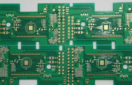
Printed Circuit Board (PCB) manufacturing involves several critical processes, one of which is reflow soldering. Reflow soldering is a key technique used to attach surface-mount components to PCBs by melting solder paste to form reliable electrical and mechanical connections. This process is widely adopted in the electronics industry due to its efficiency, precision, and scalability for mass production.
This article explores the reflow soldering process, its key stages, common challenges, and best practices to ensure high-quality solder joints in PCB assembly.
1. The Reflow Soldering Process
Reflow soldering involves heating the PCB and its components in a controlled manner to melt the solder paste, which then solidifies to form permanent connections. The process typically consists of four main stages:
1.1 Solder Paste Application
Before reflow soldering, solder paste—a mixture of tiny solder particles and flux—is applied to the PCB pads using a stencil printer. The stencil ensures precise deposition of the paste only on the designated areas where components will be placed.
1.2 Component Placement
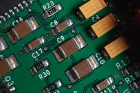
After solder paste application, surface-mount devices (SMDs) such as resistors, capacitors, and integrated circuits (ICs) are placed onto the PCB using pick-and-place machines. The tackiness of the solder paste holds components in place temporarily before reflow.
1.3 Reflow Soldering Profile
The PCB then enters a reflow oven, where it undergoes a carefully controlled temperature profile consisting of four key phases:
- Preheat/Ramp-Up Phase
- The PCB is gradually heated (typically at 1-3°C per second) to avoid thermal shock.
- Flux in the solder paste activates, removing oxides from metal surfaces to improve wetting.
- Soak/Pre-Reflow Phase
- The temperature stabilizes (usually between 150-180°C) to ensure uniform heating across the PCB.
- This phase helps evaporate solvents and prevents solder splattering.
- Reflow (Peak Temperature) Phase
- The temperature rises rapidly to the solder’s melting point (typically 217-250°C for lead-free solder).
- The solder paste melts, forming intermetallic bonds between component leads and PCB pads.
- Cooling Phase
- The PCB is cooled at a controlled rate (1-4°C per second) to solidify the solder joints.
- Rapid cooling can lead to brittle joints, while slow cooling may result in excessive intermetallic growth.
1.4 Inspection and Testing
After reflow, PCBs undergo visual inspection, automated optical inspection (AOI), or X-ray inspection to detect defects such as:
- Bridging (unintended solder connections between pads)
- Tombstoning (components standing on one end due to uneven heating)
- Cold joints (dull, brittle solder joints from insufficient heat)
- Voiding (gas pockets trapped in solder joints)
2. Types of Reflow Soldering
Different reflow soldering techniques are used based on production requirements:
2.1 Convection Reflow
- The most common method, using heated air to transfer thermal energy.
- Provides uniform heating and is suitable for high-volume production.
2.2 Infrared (IR) Reflow
- Uses infrared radiation to heat the PCB.
- Less common today due to uneven heating and shadowing effects.
2.3 Vapor Phase Reflow
- The PCB is immersed in a heated vapor (e.g., perfluoropolyether) for uniform temperature distribution.
- Highly precise but more expensive and less scalable for mass production.
2.4 Laser Reflow
- A localized soldering method using laser beams for high-precision applications.
- Ideal for sensitive components that cannot withstand oven heating.
3. Challenges in Reflow Soldering
Despite its advantages, reflow soldering presents several challenges:
3.1 Thermal Management
- Different components have varying thermal mass, leading to uneven heating.
- Large components may require a modified reflow profile to prevent cold joints.
3.2 Solder Paste Quality
- Poor solder paste consistency can cause insufficient wetting or excessive voiding.
- Flux activity must be optimized to prevent oxidation while minimizing residue.
3.3 Component Warping and Damage
- Excessive heat can damage temperature-sensitive components (e.g., LEDs, plastic connectors).
- Warping of thin PCBs may occur if heating is uneven.
3.4 Tombstoning and Misalignment
- Uneven solder paste deposition or heating can cause smaller components (e.g., 0201 resistors) to lift on one end.
3.5 Void Formation
- Voids in solder joints weaken mechanical strength and thermal conductivity.
- Causes include outgassing, poor flux activation, or improper reflow profiles.
4. Best Practices for Optimal Reflow Soldering
To mitigate challenges and ensure high-quality solder joints, manufacturers should follow these best practices:
4.1 Optimize the Reflow Profile
- Adjust heating rates, soak times, and peak temperatures based on PCB thickness and component requirements.
- Use thermocouples to validate temperature uniformity across the PCB.
4.2 Use High-Quality Solder Paste
- Select solder paste with appropriate alloy composition (e.g., SAC305 for lead-free applications).
- Store solder paste properly (refrigeration) to prevent degradation.
4.3 Ensure Proper Stencil Design
- Aperture size and stencil thickness should match component pad dimensions.
- Nano-coated stencils improve paste release for fine-pitch components.
4.4 Control the Assembly Environment
- Maintain low humidity to prevent moisture absorption in PCBs (which can cause “popcorning” in ICs).
- Use nitrogen (N₂) atmosphere in reflow ovens to reduce oxidation.
4.5 Implement Robust Inspection Methods
- Use AOI and X-ray inspection to detect hidden defects like voids or insufficient solder.
- Conduct cross-sectional analysis for critical applications (e.g., aerospace, medical devices).
5. Future Trends in Reflow Soldering
Advancements in PCB assembly continue to shape reflow soldering techniques:
- Low-Temperature Soldering: New alloys (e.g., Sn-Bi) reduce thermal stress on components.
- Smart Reflow Ovens: AI-driven ovens adjust profiles in real-time based on thermal feedback.
- Sustainability: Lead-free and halogen-free solder pastes align with environmental regulations.
Conclusion
Reflow soldering is a critical process in PCB manufacturing, enabling reliable and efficient assembly of surface-mount components. By understanding the reflow profile, addressing common challenges, and implementing best practices, manufacturers can achieve high-yield production with minimal defects. As technology evolves, innovations in solder materials, inspection methods, and thermal management will further enhance the reflow soldering process, ensuring its continued relevance in electronics manufacturing.
By optimizing each stage—from solder paste application to final inspection—engineers can produce robust PCBs that meet the demands of modern electronic devices.