Compact PCB Fab-in-a-Box: Complete DIY Circuit Lab
Key Takeaways
Building your own PCB manufacturing setup requires understanding core components that balance portability with professional results. A fab-in-a-box system typically includes transfer paper for design imprinting, copper-clad laminate as your base material, and heat-sealing foils to protect traces during etching. While commercial PCB manufacturing companies rely on industrial equipment, this compact approach lets you produce boards anywhere—ideal for prototyping or small-batch projects.
When comparing PCB manufacturing cost, DIY methods reduce expenses by 60-80% for low-volume runs. For example:
| Expense Type | Commercial Service | DIY Setup |
|---|---|---|
| Setup (Initial) | $0 | $120–$300 |
| Per Board (10cm²) | $5–$15 | $0.50–$2 |
| Lead Time | 3–7 days | 2–4 hours |
The etching phase demands precision: mix ferric chloride (or eco-friendly alternatives) in a sealed container, agitate gently, and monitor copper dissolution. Acetone removes transfer paper residues, revealing crisp traces. For those exploring a PCB manufacturing business, this system scales efficiently—batch processing 5–10 boards simultaneously with minimal space. Always prioritize ventilation and safety gear, as chemicals involved require careful handling. By mastering these steps, you gain control over design iterations and timelines typically managed by third-party vendors.
Portable PCB Lab Setup Essentials
Building a PCB manufacturing workspace in compact form requires prioritizing space efficiency and multifunctional tools. Start with a portable etching station—a heat-resistant tray, precision tweezers, and a glass container for etchant solutions like ferric chloride. Pair this with high-quality transfer paper and copper-clad laminate, ensuring clean pattern transfers for professional-grade boards.
Tip: Organize your workspace vertically using wall-mounted racks for chemicals and tools—this maximizes surface area while keeping hazardous materials secure.
While commercial PCB manufacturing companies rely on industrial equipment, your DIY setup can achieve comparable precision by focusing on material quality. For example, using laser-printed transfer paper reduces errors compared to inkjet alternatives, directly impacting PCB manufacturing cost savings. A well-optimized lab also supports small-scale PCB manufacturing business prototyping, bypassing minimum-order requirements from external suppliers.
Explore compact etching solutions that integrate storage for acetone and sealing foils, streamlining the process from design to finished board. Critical additions include a digital caliper for verifying trace widths and a ventilated enclosure to safely manage fumes—a non-negotiable for repeated use. By balancing portability with professional-grade results, your setup bridges the gap between hobbyist tools and industrial PCB manufacturing workflows.
DIY Circuit Board Fabrication Guide
To create professional-grade PCBs at home, start by understanding the core principles of pcb manufacturing. Unlike industrial pcb manufacturing companies, a DIY approach relies on accessible tools: transfer paper for transferring designs, copper-clad laminate as the base material, and sealing foils to protect critical traces. Begin by printing your circuit design onto transfer paper using a laser printer, then heat-press it onto the copper surface. This method mimics precision seen in commercial setups but at a fraction of the pcb manufacturing cost.
After transferring, submerge the board in ferric chloride or another etchant to dissolve exposed copper. Rinse with acetone to remove residual ink, revealing clean traces. While professional pcb manufacturing business operations use automated drilling, a handheld micro-drill works for prototypes. For multilayer designs, align layers meticulously—a step where commercial processes excel but DIYers can achieve accuracy with patience.
Key advantages include flexibility for rapid iterations and cost control, especially for low-volume projects. However, complex designs requiring HDI (High-Density Interconnect) may still benefit from partnering with pcb manufacturing companies. By mastering these techniques, you bridge the gap between hobbyist experimentation and industrial-grade results—all within a compact workspace.
Compact PCB Creation Kit Overview
A PCB manufacturing solution no longer requires industrial-scale equipment or specialized facilities. Modern compact kits condense essential tools into portable packages, letting you produce prototype boards with precision rivaling professional PCB manufacturing companies. These all-in-one systems typically include transfer paper for pattern application, copper-clad laminate as your base material, and sealing foils to protect critical traces during etching—components that mirror industrial processes at 1/10th the PCB manufacturing cost.
While traditional PCB manufacturing business models focus on bulk production, these kits prioritize accessibility for DIYers and small-batch creators. You’ll find pre-measured etching agents (ferric chloride or ammonium persulfate) and alignment guides to ensure consistent results, eliminating guesswork from chemical handling. The included acetone-based cleaner efficiently removes residual transfer films, leaving pristine copper surfaces for drilling and soldering.
Key advantages emerge when comparing workflow efficiency: industrial setups demand weeks for design validation, whereas compact kits enable same-day iterations. However, they’re optimized for single/double-layer designs under 6″x6″, making them impractical for complex multi-layer projects. For startups balancing PCB manufacturing cost and rapid prototyping needs, these systems bridge the gap between hobbyist tools and commercial-grade infrastructure.
Step-by-Step Home PCB Etching Process
To begin your PCB manufacturing journey at home, start by preparing your design. Print your circuit layout onto transfer paper using a laser printer, ensuring high contrast for precise pattern replication. Next, clean the copper laminate with acetone to remove oxidation, then align and press the transfer paper onto the surface using a laminator or household iron. Heat activates the toner, bonding it firmly to the copper.
Once cooled, submerge the board in warm water to dissolve the paper backing, leaving only the toner mask. Prepare your etchant solution (ferric chloride or vinegar-hydrogen peroxide mix) in a plastic tray, then agitate the board gently until all exposed copper dissolves—this typically takes 10–20 minutes. Rinse thoroughly to halt etching, then use acetone again to strip the toner, revealing your pristine copper traces.
While commercial PCB manufacturing companies rely on industrial equipment, this method drastically reduces PCB manufacturing cost for prototypes. For multi-layer designs or high-volume needs, outsourcing to a PCB manufacturing business remains practical, but for hobbyists, mastering this process unlocks full control over rapid iterations. Always prioritize ventilation and safety gear when handling chemicals, and store etchant properly for reuse.
Professional-Grade DIY Electronics Tools
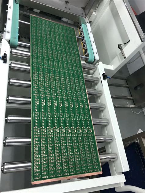
When building your own PCB manufacturing setup, professional-grade tools bridge the gap between hobbyist experiments and industrial-quality results. Unlike basic kits, these tools prioritize precision and repeatability, mirroring techniques used by established PCB manufacturing companies. You’ll need a temperature-controlled laminator for consistent transfer paper bonding, a high-resolution UV exposure unit for intricate traces, and a programmable etching tank to automate chemical processes. While PCB manufacturing cost for industrial-scale production often exceeds DIY budgets, compact systems let you achieve similar accuracy at a fraction of the price.
For example, rotary engravers with micron-level control can replace laser-cut stencils, while desktop solder paste dispensers ensure clean component placement. These tools not only streamline prototyping but also equip you to handle complex designs—a critical skill if you ever scale into a small PCB manufacturing business. Pair them with quality materials like FR-4 copper laminates and industrial-grade etchants to minimize errors. By integrating professional methods into your workflow, you transform a portable lab into a capable production environment, ready for everything from IoT modules to high-frequency circuits.
Mobile Circuit Lab Components Explained
A portable PCB manufacturing setup requires precisely curated tools that balance professional-grade results with compact usability. At its core, you’ll need transfer paper for transferring designs onto copper-clad laminates—a critical step that replaces industrial printers used by PCB manufacturing companies. The kit’s copper laminate sheets serve as your blank canvas, while sealing foils protect non-etched areas during chemical processing.
Completing the system are two chemical agents: etchant solution (typically ferric chloride) to remove excess copper and acetone for cleaning residual transfer paper. These components mirror scaled-down versions of tools found in traditional PCB manufacturing business operations but eliminate reliance on bulk equipment.
What makes this setup uniquely efficient is its cost-effectiveness—a PCB manufacturing cost reduction of 60-80% compared to outsourcing small batches. By combining these elements, you gain control over prototyping timelines without sacrificing precision. The modular design ensures all components fit in a briefcase-sized container, making it ideal for field engineers or makerspaces needing on-demand production.
When selecting materials, prioritize UV-resistant sealing foils and high-resolution transfer paper to achieve clean traces comparable to commercial standards. This approach bridges the gap between DIY experimentation and professional PCB manufacturing, empowering you to iterate designs anywhere.
Transfer Paper Techniques for PCB Design
Mastering transfer paper techniques unlocks precise pattern replication for DIY PCB manufacturing, eliminating reliance on commercial PCB manufacturing companies. Begin by printing your design onto heat-resistant transfer paper using a laser printer—toner acts as an etch-resistant mask. Align the printed side against a cleaned copper laminate, then apply even heat (120-150°C) with a laminator or household iron. The heat transfers toner to the copper, creating a durable blueprint for etching.
For complex designs, double-check alignment before pressing to avoid mismatched traces. After transferring, gently peel the paper while the surface is warm, ensuring no toner lifts. Imperfections can be corrected with a fine-tip permanent marker—a cost-saving alternative to professional-grade tools used in large-scale PCB manufacturing business operations.
This method reduces PCB manufacturing cost by 60-80% compared to outsourcing, ideal for prototyping or low-volume projects. Store unused transfer sheets in a cool, dry place to prevent premature adhesion. Pair these techniques with precise etching (covered later) to achieve results rivaling industrial processes—all within your compact lab setup.
Complete Etching Solutions for Beginners
Mastering PCB manufacturing at home starts with understanding etching fundamentals. While professional PCB manufacturing companies rely on industrial equipment, your compact setup uses transfer paper, copper laminate, and sealing foils to achieve similar results. Begin by transferring your design onto the copper-clad board using heat or pressure. Submerge it in etchant solution (ferric chloride or ammonium persulfate) to dissolve unprotected copper, leaving only your circuit traces.
To optimize PCB manufacturing cost, control etchant concentration and reuse it until saturation. Rinse the board with water, then remove residual toner using acetone—this step ensures clean contacts for components. For beginners, pre-measured etching kits simplify the process, eliminating guesswork.
Though DIY methods can’t match the precision of large-scale PCB manufacturing business operations, they offer flexibility for prototyping. Adjust exposure times or etchant temperatures to refine results. Always prioritize safety: wear gloves and work in ventilated spaces. By mastering these basics, you’ll bridge the gap between hobbyist experiments and professional-grade outputs—all within your portable lab.
Compact PCB Creation Kit Overview
A modern PCB manufacturing solution no longer requires industrial-scale facilities. With a compact footprint and precisely curated components, these portable kits condense essential fabrication tools into a single package. You’ll find transfer paper for transferring designs, copper laminate boards as your substrate, and sealing foils to protect critical traces during etching—all designed to replicate processes used by professional PCB manufacturing companies at a fraction of the PCB manufacturing cost.
The core advantage lies in eliminating reliance on external suppliers. Whether prototyping a new circuit or troubleshooting designs, you maintain full control over timelines—a critical factor for small-scale PCB manufacturing business operations. Kits prioritize user-friendly workflows: align your printed design with the copper board, apply heat for transfer, then immerse in etchant to reveal conductive paths. Acetone effortlessly removes residual toner, leaving clean traces ready for drilling.
This brings us to cost efficiency. Traditional outsourcing often incurs minimum order fees and shipping delays. By internalizing production, you reduce per-unit expenses while enabling rapid iterations—ideal for startups or hobbyists refining designs. The scalable nature of these kits ensures they grow with your needs, whether you’re producing five boards or fifty.
Next, we’ll explore how to execute each fabrication step with precision, ensuring professional-grade results from your DIY setup.
Conclusion
The PCB manufacturing landscape has evolved to accommodate both industrial-scale production and personal experimentation. While traditional PCB manufacturing companies excel at high-volume orders, the affordable PCB manufacturing cost of compact Fab-in-a-Box systems democratizes prototyping for makers and engineers. By integrating transfer paper, copper laminates, and etching tools into a portable kit, you gain the flexibility to iterate designs without relying on external suppliers—a critical advantage for refining PCB manufacturing business concepts or testing functional prototypes.
This self-contained approach not only reduces lead times but also sharpens your understanding of material interactions and process optimization. Whether you’re troubleshooting circuit layouts or exploring niche applications, the ability to produce boards on-demand fosters creativity while keeping costs predictable. For startups and hobbyists alike, mastering these techniques bridges the gap between DIY experimentation and professional-grade output, proving that PCB manufacturing isn’t confined to factory floors. With practice, your compact lab can rival the precision of commercial services, turning ambitious ideas into tangible electronics—one etched board at a time.
FAQs
How does a compact PCB Fab-in-a-Box compare to traditional pcb manufacturing methods?
While traditional pcb manufacturing companies rely on industrial equipment, this portable kit simplifies prototyping. You gain control over pcb manufacturing cost by eliminating outsourcing fees, though it’s ideal for small-scale projects rather than mass production.
What components are critical for DIY pcb fabrication?
Your kit should include transfer paper, copper-clad laminate, and sealing foils. These materials, combined with household chemicals like etchant and acetone, replicate core steps used in professional pcb manufacturing business workflows.
Can beginners achieve reliable results with this method?
Yes, but precision matters. Align transfer paper carefully to avoid circuit errors, and monitor etching times closely. For complex designs, partnering with pcb manufacturing companies ensures higher accuracy.
How does cost-effectiveness scale with project size?
DIY kits reduce pcb manufacturing cost for prototypes or single boards. However, for batches exceeding 10 units, traditional pcb manufacturing becomes more economical due to bulk material discounts.
What safety precautions are necessary?
Always wear gloves and goggles when handling etchants. Store chemicals in labeled containers, and dispose of waste responsibly—practices aligned with professional pcb manufacturing business safety standards.
Ready to Scale Your PCB Projects?
For advanced designs or larger batches, explore professional solutions from trusted pcb manufacturing companies. Click here to request a quote and compare costs for your next project.
