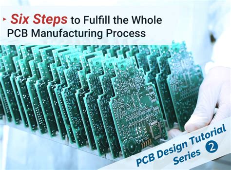
PCB Manufacturing Automation: Streamlining Design to Assembly
Key Takeaways
When optimizing PCB manufacturing workflows, automation bridges the gap between design and production. By automating processes like Gerber file conversion and component placement, PCB manufacturing companies minimize human error while accelerating timelines. For instance, robotic assembly lines ensure sub-millimeter precision in placing components, directly reducing PCB manufacturing cost through fewer defects and material waste.
"Investing in integrated automation systems allows your PCB manufacturing business to handle complex designs without compromising speed or quality."
Advanced tools like AI-driven inspection systems scan boards for defects at microscopic levels, ensuring compliance with industry standards. This not only streamlines the Gerber-to-manufacturing workflow but also enables smarter resource allocation. Additionally, machine learning algorithms analyze historical data to predict potential bottlenecks, allowing you to adjust production schedules proactively.
By adopting end-to-end automation, you eliminate manual handoffs between design, fabrication, and testing phases. Smart factories leverage real-time monitoring to slash prototyping cycles, giving your operations a competitive edge. Whether you’re scaling production or refining prototypes, automation ensures consistency across every batch—critical for meeting tight deadlines without sacrificing reliability.
Automating PCB Design File Conversion Processes
When managing PCB manufacturing workflows, converting design files like Gerber or ODB++ into machine-readable formats has traditionally required manual intervention, creating bottlenecks. By automating these conversions, PCB manufacturing companies reduce human error and accelerate prototyping cycles. Modern tools parse design files, validate layer alignments, and generate assembly instructions autonomously—cutting setup time by up to 70%.
For example, automated systems detect mismatches between schematic layouts and fabrication requirements, flagging issues like insufficient copper clearances before production begins. This proactive approach minimizes costly revisions, directly lowering PCB manufacturing cost for high-volume orders.
| Manual Conversion | Automated Conversion |
|---|---|
| 8–12 hours per design | 1–2 hours per design |
| 15% error rate | <2% error rate |
| Limited scalability | Seamless batch processing |
Integrating these systems into your PCB manufacturing business ensures consistency across clients’ projects, whether you’re handling rigid, flex, or HDI boards. Advanced platforms even adapt to evolving standards, such as IPC-2581, ensuring compatibility with global suppliers.
By implementing automated file conversion tools, you eliminate redundant tasks while maintaining precision—critical for meeting tight deadlines in industries like automotive or aerospace. This shift not only streamlines workflows but also frees engineering teams to focus on innovation rather than administrative overhead.
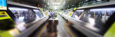
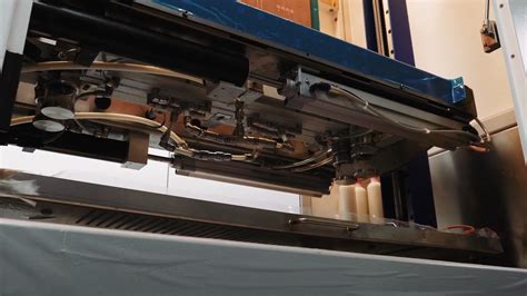
Robotic Assembly Lines Revolutionizing PCB Production
When optimizing your PCB manufacturing workflow, robotic assembly lines offer unparalleled consistency in handling complex tasks. Modern systems integrate high-speed pick-and-place robots, automated soldering arms, and precision-guided conveyor belts, enabling PCB manufacturing companies to scale production without compromising quality. These systems excel at placing micro-components with sub-millimeter accuracy, directly addressing challenges like PCB manufacturing cost reduction and yield improvement.
By replacing manual labor in repetitive tasks, robotics minimize human error—critical for multilayer boards or designs with fine-pitch components. Advanced vision systems paired with force-sensitive actuators ensure components align perfectly, even in high-mix, low-volume scenarios common in the PCB manufacturing business. This shift not only accelerates throughput but also creates flexibility to adapt to rapid design changes, a key advantage in fast-paced markets.
For businesses, the ROI extends beyond speed: automated lines reduce rework rates by up to 60%, lowering long-term operational expenses. As you transition toward smart factories, integrating these systems with AI-driven inspection tools (covered later) forms a cohesive ecosystem—transforming how design intent translates into physical boards.
AI-Driven Quality Control in Circuit Board Fabrication
When optimizing PCB manufacturing workflows, ensuring precision at every stage is non-negotiable. This is where AI-driven systems step in, transforming how PCB manufacturing companies identify and address defects. By leveraging machine learning algorithms and high-resolution imaging, these systems analyze thousands of circuit patterns in real time, detecting micro-faults like solder bridging or misaligned traces that human inspectors might overlook.
The integration of AI not only elevates accuracy but also directly impacts PCB manufacturing cost. Automated defect detection reduces material waste and minimizes rework, allowing businesses to allocate resources more efficiently. For instance, a single undetected flaw in a prototype could cascade into costly delays during mass production. By catching errors early, predictive analytics help streamline timelines, ensuring faster turnaround without compromising quality.
For PCB manufacturing business models focused on scalability, AI-powered quality control acts as a competitive differentiator. These systems adapt to evolving design complexities, learning from historical data to refine inspection criteria over time. Whether you’re producing high-density interconnect boards or flexible circuits, the result is a consistently reliable product that meets stringent industry standards. By automating this critical phase, manufacturers bridge the gap between robotic assembly lines and final testing, creating a seamless, end-to-end production ecosystem.
Streamlining Gerber-to-Manufacturing Workflow Automation
Automating the transition from Gerber files to physical PCB production eliminates bottlenecks that traditionally slow down pcb manufacturing. By implementing specialized software to interpret design data, you reduce manual interpretation errors while accelerating timelines—critical factors for pcb manufacturing companies competing in fast-paced markets. These systems automatically validate layer alignment, drill patterns, and copper traces, flagging inconsistencies before they escalate into costly rework.
Real-time adjustments to fabrication parameters ensure compatibility with your factory’s equipment, whether you’re producing high-density interconnect boards or flexible circuits. This seamless integration between design and manufacturing phases directly impacts pcb manufacturing cost, as automated workflows minimize material waste and optimize machine utilization. For example, intelligent nesting algorithms arrange multiple board designs on a single panel, maximizing substrate efficiency.
The ripple effect extends to the broader pcb manufacturing business, where standardized automation protocols enable faster scaling. Instead of relying on fragmented processes, unified platforms synchronize tasks like solder mask application and silkscreen printing, reducing idle time between production stages. By bridging the gap between digital designs and physical assembly, automated workflows ensure your operations stay agile—ready to adapt to evolving client demands without sacrificing precision.
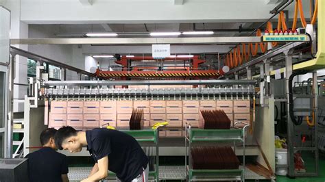
Precision Enhancement Through Automated Component Placement
When optimizing PCB manufacturing workflows, achieving micron-level accuracy in component placement remains critical. Modern automated pick-and-place systems leverage robotic arms with vision-guided alignment, ensuring components are positioned within ±25 microns of their designated locations. This precision-first approach minimizes human error while accommodating complex designs with high-density interconnects—a key advantage for PCB manufacturing companies handling advanced IoT or aerospace applications.
By integrating real-time feedback loops, these systems dynamically adjust placement parameters based on thermal expansion or board warpage detected during assembly. Such adaptability directly impacts PCB manufacturing cost by reducing scrap rates—studies show automated lines achieve first-pass yields exceeding 99.2%, compared to 92-95% in manual setups. For PCB manufacturing business models prioritizing rapid scalability, this technology eliminates bottlenecks in mixed-batch production, allowing seamless transitions between prototype runs and full-scale volumes without recalibration delays.
The synergy between machine learning algorithms and servo-controlled placement heads further refines positional accuracy over time. As systems analyze historical placement data, they predictively compensate for mechanical drift—ensuring consistent precision even during 24/7 operation cycles. This self-optimizing capability transforms component placement from a static process into an intelligent, error-resistant workflow, reinforcing automated assembly as the backbone of modern PCB fabrication.
Smart Factories: Reducing Timelines in PCB Prototyping
In modern PCB manufacturing, smart factories are redefining prototyping efficiency by integrating IoT-enabled systems and real-time data analytics. By automating workflows from design validation to material sourcing, these facilities compress timelines that once bottlenecked PCB manufacturing companies. For instance, predictive maintenance algorithms monitor equipment health preemptively, minimizing downtime during critical prototyping phases. Advanced digital twins simulate board behavior under varying conditions, allowing engineers to iterate designs without physical rework—a game-changer for managing PCB manufacturing cost.
The shift to smart factories also streamlines collaboration between design and production teams. Cloud-based platforms sync updates instantly, ensuring Gerber files reflect the latest revisions before assembly begins. Robotic arms equipped with machine vision handle micro-component placement with micron-level accuracy, reducing errors that traditionally delayed prototypes. For PCB manufacturing business models prioritizing speed-to-market, this agility translates to faster client feedback cycles and improved competitiveness. By eliminating manual handoffs and leveraging data-driven decision-making, smart factories cut prototyping lead times by up to 60%, a critical advantage in industries where time-to-production dictates market success.
Integrated Systems for End-to-End PCB Manufacturing
Modern PCB manufacturing thrives on seamless integration across design, fabrication, and assembly stages. By adopting integrated systems, PCB manufacturing companies eliminate manual handoffs between departments, reducing errors and delays. These platforms automatically translate design files—like Gerber data—into machine-readable instructions, ensuring precision in trace routing and layer alignment. For example, automated workflows synchronize component procurement with production schedules, optimizing PCB manufacturing cost by minimizing material waste and idle time.
Advanced systems also bridge fabrication and assembly through real-time data sharing. Sensors on robotic pick-and-place machines adjust component positioning based on live feedback from inspection cameras, enhancing yield rates. This closed-loop automation is particularly valuable for PCB manufacturing business models that handle high-mix, low-volume orders, where flexibility matters. By unifying supply chain management with factory-floor operations, businesses can dynamically reroute orders during bottlenecks—a critical advantage in meeting tight deadlines.
Ultimately, integrated ecosystems empower you to scale operations without compromising quality. Whether prototyping or mass-producing boards, end-to-end automation ensures every phase aligns with your technical specifications and budgetary constraints.
Machine Learning in PCB Defect Detection and Testing
When optimizing PCB manufacturing workflows, defect detection remains a critical bottleneck. Traditional manual inspections struggle to keep pace with modern production speeds, often leading to overlooked flaws or delayed timelines. This is where machine learning (ML) steps in, analyzing thousands of circuit patterns in real time to identify microscopic defects—from soldering inconsistencies to trace misalignments—with unmatched precision. By training algorithms on historical defect data, PCB manufacturing companies can predict and flag errors before boards move to assembly, reducing PCB manufacturing cost through fewer material rejects and reworks.
ML-powered systems adapt dynamically, learning from each production cycle to refine detection thresholds. For instance, they can distinguish between acceptable variations in copper traces and genuine faults, minimizing false positives that stall workflows. This capability becomes especially valuable in high-volume runs, where even minor improvements in accuracy translate to significant savings. By integrating ML into quality control, your PCB manufacturing business not only accelerates testing phases but also builds trust through consistently reliable outputs. The result? Smoother transitions from prototyping to mass production, with fewer disruptions and higher yields.
Conclusion
As you navigate the evolving landscape of PCB manufacturing, it becomes clear that automation isn’t just an option—it’s a necessity for staying competitive. Modern PCB manufacturing companies are leveraging integrated systems to bridge design and production, minimizing errors while accelerating timelines. By automating processes like Gerber file conversion and component placement, businesses reduce PCB manufacturing cost through improved resource allocation and fewer material redundancies.
The shift toward smart factories ensures that AI-driven quality checks and robotic assembly lines work in tandem, delivering precision at scale. For your PCB manufacturing business, this means shorter prototyping cycles and the ability to meet tighter deadlines without compromising on reliability. Advanced machine learning algorithms further refine defect detection, cutting down post-production rework and enhancing customer trust.
Ultimately, the goal is to create a seamless workflow where design files transition effortlessly into physical boards. By prioritizing automation, you position your operations to adapt to market demands while maintaining control over PCB manufacturing cost and quality. Whether you’re scaling production or refining prototypes, the integration of these technologies ensures your business remains agile in an industry where efficiency defines success.
FAQs
How does automation impact lead times in PCB manufacturing?
Automated systems streamline processes from PCB manufacturing design to assembly, reducing manual interventions. This cuts production cycles by 30–50%, enabling faster prototyping and delivery—critical for meeting tight project deadlines.
What cost factors should you consider when adopting automation?
While upfront investments in robotics and AI-driven tools affect PCB manufacturing cost, long-term savings from reduced errors, material waste, and labor often offset initial expenses. Automated workflows also improve scalability for growing PCB manufacturing business operations.
Can small-scale PCB manufacturing companies benefit from automation?
Yes. Modular automation solutions allow smaller PCB manufacturing companies to integrate specific tools, like AI-based quality checks or automated component placement, without overhauling entire production lines. This flexibility balances efficiency gains with budget constraints.
How does automation improve precision in circuit board fabrication?
Advanced vision systems and machine learning algorithms detect micron-level defects during PCB manufacturing, ensuring consistent quality. Robotic arms achieve sub-millimeter accuracy in component placement, minimizing rework and enhancing product reliability.
What challenges arise when transitioning to automated workflows?
Integration complexity and staff training are common hurdles. However, partnering with experienced PCB manufacturing providers simplifies adoption through tailored software-hardware solutions and technical support.
Ready to Optimize Your PCB Production?
Explore how Andwin PCB’s automated solutions can transform your workflows. Click here to learn more about our services.