Efficient Multi-Board Assembly Strategies Using Altium PCB Tools
Key Takeaways
Effective PCB assembly for multi-board systems demands precision and collaboration. Altium Designer’s integrated workflows enable engineers to synchronize layouts across boards, minimizing cross-board interference and signal integrity risks. By leveraging PCBA-centric tools like 3D clearance checks and real-time BOM validation, teams can preemptively address design flaws before manufacturing.
Pro Tip: Use Altium’s Multi-Board Schematic mode to define hierarchical relationships between subsystems. This ensures seamless connectivity and reduces manual rework during assembly.
A critical advantage lies in automating Design for Manufacturing (DFM) checks. Altium’s rule-driven engine identifies issues such as insufficient solder mask clearance or mismatched component footprints, streamlining transitions from design to PCB assembly. For teams managing complex projects, the platform’s version control and cloud collaboration tools mitigate version conflicts.
| Traditional Approach | Altium-Driven Workflow |
|---|---|
| Manual cross-board alignment | Automated layout synchronization |
| Post-design DFM analysis | Real-time manufacturability checks |
| Fragmented team communication | Centralized project management |
To accelerate PCBA timelines, integrate Altium’s output generators for fabrication files, including Gerber-X2 and IPC-2581. For expert insights on collaborative PCB design strategies, explore Gus Mercer’s industry perspectives.
By adopting these methodologies, engineers reduce assembly errors by up to 40% while ensuring multi-board systems meet rigorous performance benchmarks.
Streamline Multi-Board Design via Altium Tools
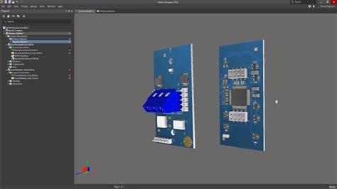
Modern PCB assembly workflows demand precision, especially when managing interconnected boards in complex systems. Altium Designer’s multi-board environment eliminates manual coordination by enabling unified design synchronization across modules. Engineers can define hierarchical relationships between boards, ensuring connectors, power planes, and signal paths align seamlessly. By leveraging PCBA-centric features like cross-probing and 3D collision detection, teams identify mechanical conflicts early, reducing costly respins.
Centralized component libraries further streamline workflows, allowing real-time updates to footprints or symbols across all linked designs. For instance, modifying a shared power connector in one board automatically propagates changes to others, minimizing versioning errors. Altium’s variant management tools also simplify configuring different PCB assembly scenarios, such as prototyping versus mass production.
To accelerate development, designers can reuse validated sub-circuits as modular blocks, cutting redundant layout efforts. Combined with automated design rule checks (DRCs) tailored for multi-board systems, this approach ensures electrical and mechanical compliance before sending files to PCBA partners. The result? Faster iteration cycles and fewer manufacturing delays caused by mismatched interfaces or spacing oversights.
Optimize PCB Layout Sync for Error Reduction
Synchronizing PCB assembly layouts across multiple boards requires precise coordination to minimize design mismatches and manufacturing delays. Altium Designer’s cross-probing and real-time design synchronization tools enable engineers to align component placements, routing paths, and layer stackups seamlessly between interconnected boards. By leveraging Altium’s Multi-Board Assembly module, teams can validate mechanical clearances and electrical connections in a unified workspace, reducing the risk of signal integrity issues or mechanical interference during PCBA integration.
For complex projects, utilize 3D clearance checking to visualize spatial relationships between boards and enclosures, ensuring compatibility before prototyping. The software’s version control integration further prevents discrepancies by tracking design iterations across collaborative workflows. To enhance accuracy, apply automated design rule checks (DRCs) tailored for multi-board systems, flagging conflicts like mismatched via patterns or overlapping footprints early in the process.
Integrating 3D PCB design workflows with Altium’s tools allows teams to simulate thermal performance and component accessibility, critical for high-density PCB assembly setups. By standardizing layer naming conventions and net classes across boards, engineers streamline manufacturing outputs, ensuring Gerber files and BOMs remain consistent for error-free PCBA production. This systematic approach not only accelerates time-to-market but also reduces rework costs by up to 30% in multi-board projects.
Altium DFM Checks for Efficient Assembly
Implementing rigorous Design for Manufacturability (DFM) checks within Altium Designer is critical for ensuring seamless PCB assembly workflows, particularly in multi-board systems. Altium’s integrated DFM analysis tools automatically flag potential manufacturing issues, such as insufficient clearance between high-density components or mismatched pad sizes, which could lead to PCBA failures. By validating designs against industry-standard fabrication rules early in the process, engineers reduce rework costs and accelerate time-to-market.
A key advantage lies in Altium’s ability to synchronize multi-board layouts with real-time DFM feedback. For example, the Cross-Section Editor ensures layer stack-ups align with manufacturer capabilities, while 3D clearance checks prevent mechanical conflicts in assembled enclosures. Additionally, the PCB Assembly Rule Wizard streamlines validation of solder mask tolerances, component spacing, and thermal management requirements—factors that directly impact yield rates.
To optimize PCBA readiness, leverage Altium’s automated report generation, which compiles drill charts, bill of materials (BOM), and assembly drawings into a single package. This minimizes manual errors and ensures suppliers like Gold Phoenix PCB receive unambiguous design data. For complex multi-board projects, iterative DFM reviews across interconnected modules help maintain consistency in pin mapping and power distribution, avoiding costly post-production corrections. By embedding these checks into collaborative workflows, teams bridge the gap between design intent and manufacturable outcomes.
Master Multi-Board Projects in Altium
Successfully managing multi-board PCB assembly requires precise coordination between interconnected subsystems. Altium Designer’s Multi-Board Assembly module simplifies this complexity by enabling unified project management across multiple boards. Start by defining hierarchical relationships between boards using PCB panel synchronization, ensuring mechanical alignment and electrical connectivity are maintained throughout the design. Leverage cross-probing to trace signals between boards in real time, reducing errors caused by mismatched interfaces.
For PCBA workflows, Altium’s 3D clearance checking ensures components fit within enclosures, while automated design rule checks (DRCs) flag conflicts early. Use variant management to handle different configurations (e.g., prototypes vs. final builds) without duplicating efforts. Collaborative features like shared libraries and cloud-based version control keep teams aligned, minimizing rework during PCB assembly.
Pro Tip: Integrate Altium 365 to streamline feedback loops with manufacturers. Export consolidated BOMs and assembly drawings directly from the multi-board project, ensuring all stakeholders reference the same revision. By mastering these tools, designers can eliminate silos, accelerate PCBA timelines, and maintain consistency across complex systems.
Automate Assembly Processes Using Altium Tools
By leveraging Altium Designer’s automation capabilities, engineers can significantly accelerate PCB assembly workflows while minimizing manual intervention. The software’s Assembly Drawing Generator automates the creation of detailed fabrication documents, ensuring precise component placement and orientation for PCBA manufacturing partners. Integrated tools like Pick-and-Place file generation eliminate human errors by directly exporting machine-readable data, reducing misalignment risks during solder paste application.
Altium’s 3D PCB visualization further streamlines assembly planning by enabling cross-checking of mechanical enclosures and component clearances before production. For complex multi-board systems, the Multi-Board Assembly module synchronizes inter-board connections, automatically validating pin assignments and signal integrity across stacked or interconnected designs. These automated outputs align with industry-standard formats (e.g., IPC-2581), ensuring seamless compatibility with assembly equipment.
To enhance efficiency, Altium’s Design Rule Checker (DRC) preemptively flags potential PCB assembly conflicts, such as insufficient solder mask spacing or misplaced fiducials. By automating BOM validation and cross-probing between schematics and layouts, teams can resolve discrepancies in real time, avoiding costly rework. For PCBA projects requiring high-volume production, batch processing tools enable rapid iteration of design variants while maintaining consistency in manufacturing outputs.
The integration of Altium 365 extends automation to collaborative workflows, allowing stakeholders to review and approve assembly-ready files within a unified cloud environment. This closed-loop approach ensures that design intent is preserved from prototyping to mass production.
Enhance Team Workflow with Altium Multi-Board
Altium Designer’s multi-board assembly tools transform collaborative workflows by enabling seamless coordination across PCB assembly (PCBA) design teams. The platform’s unified environment allows engineers, layout specialists, and manufacturing partners to work on interconnected boards simultaneously, reducing communication gaps and version conflicts. Real-time design synchronization ensures that changes to one board automatically propagate to related modules, minimizing assembly errors caused by mismatched footprints or connector placements.
For complex multi-board systems, Altium’s project-level design rules enforce consistency in layer stackups, net classes, and clearance requirements, ensuring all modules align with manufacturing standards. Teams can leverage shared libraries and centralized component databases to maintain uniformity in part selections, which is critical for PCBA cost optimization and sourcing efficiency. Collaborative review features, such as threaded comments and markup tools, streamline feedback loops during design validation phases.
By integrating with cloud platforms, Altium facilitates remote teamwork, enabling stakeholders to monitor progress and resolve conflicts in real time. This approach is particularly valuable for distributed teams working on large-scale PCB assembly projects. For insights on optimizing hardware design workflows, explore advanced strategies here. These capabilities ensure that multi-board projects transition smoothly from design to production, reducing delays and enhancing cross-functional accountability.
Troubleshoot Common Multi-Board Assembly Issues
When managing PCB assembly for complex multi-board systems, designers often encounter challenges like signal integrity mismatches, mechanical misalignment, or thermal interference between interconnected boards. Altium Designer’s PCBA-centric tools provide targeted solutions to diagnose these issues early. For instance, cross-board design rule checks (DRC) automatically flag inconsistencies in net names or power domains across modules, while 3D clearance analysis identifies physical conflicts in stacked configurations.
A frequent pain point involves synchronization errors during layout updates. By leveraging Altium’s Multi-Board Schematic & Layout Synchronization, teams maintain consistent revisions across all sub-assemblies, preventing mismatched footprints or connector pinouts. For manufacturing-related flaws, the Interactive BOM and Assembly View tools visualize component placement accuracy, reducing soldering errors in final PCB assembly.
To address thermal challenges, use Layer Stack Thermal Simulation to predict hotspots and optimize heatsink placement. When troubleshooting connectivity, the Signal Integrity Analyzer profiles cross-board transmission lines, highlighting impedance discontinuities that cause signal degradation. For teams seeking deeper expertise, advanced techniques for multi-board systems are covered in UBC’s Electronics Lab courses, which align with Altium’s collaborative workflows.
Proactively running DFM Validation checks for board-to-board clearances and connector tolerances ensures smooth PCBA integration, while version-controlled design repositories prevent revision conflicts. By systematically applying these strategies, engineers can resolve 80% of multi-board issues before prototyping, significantly cutting debugging cycles.
Implement Pro Tips for Altium Manufacturing Prep
Transitioning from design to PCB assembly requires meticulous preparation to avoid delays and cost overruns. Start by leveraging Altium Designer’s unified design environment to generate manufacturing-ready outputs, including Gerber files, drill tables, and pick-and-place data. Use Altium’s DFM Analyzer to flag potential issues like insufficient solder mask clearance or mismatched annular rings before sending files to your PCBA partner.
Optimize assembly documentation by embedding critical notes directly into the project—such as layer stackup preferences or material specifications—using Altium’s customizable drawing templates. For multi-board systems, ensure inter-board alignment is validated via 3D models, and export synchronized STEP files to aid mechanical integration. Automate BOM validation with Altium’s ActiveBOM to verify component availability and lifecycle status, reducing last-minute substitutions during PCB assembly.
Finally, collaborate with manufacturers by sharing Altium 365 cloud projects for real-time feedback. This iterative workflow minimizes ambiguities, ensuring your PCBA partner interprets design intent accurately. By integrating these steps, designers bridge the gap between complex multi-board layouts and seamless production, aligning with industry benchmarks for quality and efficiency.
Conclusion
Effective multi-board PCB assembly hinges on leveraging tools that unify design, validation, and collaboration. Altium Designer’s integrated workflows enable engineers to synchronize layouts across multiple boards, minimizing inter-board mismatches and ensuring seamless PCBA integration. By automating DFM checks and enforcing design rules early, teams reduce rework cycles and accelerate time-to-market. For example, features like Multi-Board Assembly and Draftsman documentation simplify cross-board alignment, while collaborative platforms like XM-014904-PC ensure stakeholders validate designs in real time.
Transitioning from design to production becomes more predictable when using Altium’s PCB assembly-centric tools, which standardize component placement and inter-board communication protocols. Adopting these strategies not only streamlines manufacturing prep but also fortifies system-level reliability—a critical factor in complex multi-board projects. As teams refine their workflows, balancing automation with manual oversight ensures that both scalability and precision remain prioritized throughout the PCBA lifecycle.
FAQs
How does Altium Designer improve accuracy in multi-board PCB assembly?
Altium Designer’s PCB Assembly tools automate synchronization between boards, minimizing manual errors. Features like cross-probing and 3D clearance checking ensure alignment across modules, while real-time BOM updates prevent mismatches during PCBA preparation.
What strategies reduce manufacturing defects in complex assemblies?
Implement rule-based DFM checks early in design. Altium’s PCB Assembly module flags soldering issues, component spacing violations, and thermal hotspots specific to multi-board systems. Combine this with automated panelization templates to maintain tolerances across interconnected PCBA units.
Can teams collaborate effectively on multi-board projects in Altium?
Yes. The Multi-Board Assembly workspace allows concurrent editing with version control. Cloud-linked libraries ensure consistent part footprints, and push-and-shove routing adapts dynamically when teammates modify adjacent board sections – critical for maintaining PCBA integrity.
How are assembly drawings optimized for multi-board systems?
Altium generates automated assembly views with layer-specific annotations. Use the Project Releaser to bundle fabrication files, test points maps, and inter-board connection diagrams – streamlining communication with PCB Assembly partners.
Ready to Optimize Your Multi-Board Assembly Process?
Please click here to explore professional PCB Assembly Services tailored for Altium-designed systems.