Mastering PCB Assembly & Soldering for High-Performance Electronics
Key Takeaways
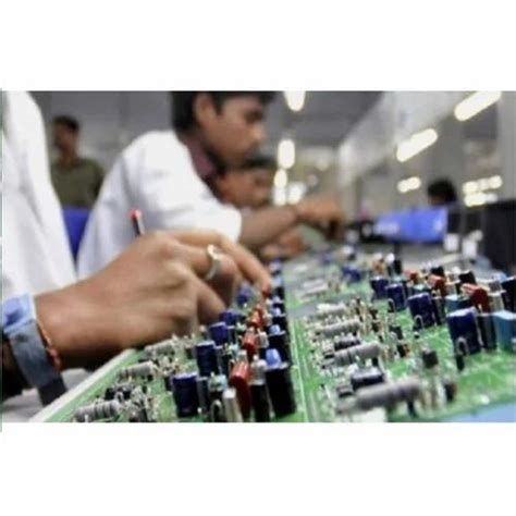
Successful PCB assembly and soldering rely on understanding critical technical and procedural elements. PCBA (Printed Circuit Board Assembly) demands precision in component placement, solder application, and thermal management to ensure high-performance outcomes. Key factors include adherence to quality standards like IPC-A-610 and ISO 9001, which govern solder joint integrity and component alignment.
Advanced equipment, such as automated pick-and-place machines and reflow ovens, enhances consistency in high-volume production. For specialized applications, selective soldering systems minimize thermal stress on sensitive components. Below is a comparison of common soldering methods:
| Method | Applications | Advantages | Limitations |
|---|---|---|---|
| Wave Soldering | Through-hole components | High throughput | Limited to single-side PCBs |
| Reflow Soldering | Surface-mount devices | Precision temperature control | Requires solder paste stencils |
Optimizing PCB assembly involves balancing speed with accuracy, particularly when handling fine-pitch ICs or BGAs (Ball Grid Arrays). Rigorous testing protocols, including AOI (Automated Optical Inspection) and X-ray analysis, identify defects early, reducing rework costs. By integrating PCBA best practices—such as proper flux application and controlled cooling rates—manufacturers achieve reliable electronics that meet stringent industry demands.
PCB Assembly Essentials for High-Performance Electronics
Effective PCB assembly forms the backbone of modern electronics manufacturing, particularly for applications demanding precision and reliability. At its core, PCBA (Printed Circuit Board Assembly) integrates component placement, soldering, and testing to ensure optimal functionality. High-performance systems require meticulous attention to material selection, thermal management, and process control to mitigate risks like signal interference or component failure.
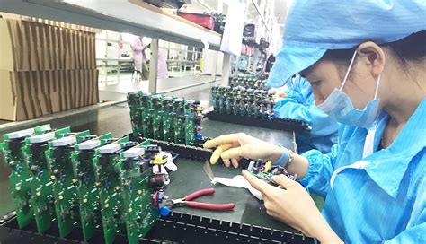
A critical factor lies in aligning PCB assembly workflows with industry-specific requirements. For instance, aerospace or medical devices often necessitate mil-spec soldering or cleanroom environments to meet stringent quality benchmarks. Advanced techniques such as surface-mount technology (SMT) and through-hole assembly must be tailored to component density and board complexity. Additionally, automated systems like pick-and-place machines and reflow ovens enhance consistency while reducing human error.
Quality assurance protocols, including automated optical inspection (AOI) and X-ray testing, further validate solder joint integrity and alignment. By prioritizing PCBA precision, manufacturers can achieve repeatable outcomes for high-frequency or high-power applications. This foundational rigor not only supports device longevity but also streamlines scalability for mass production.
Precision Soldering in PCB Manufacturing
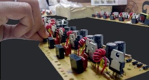
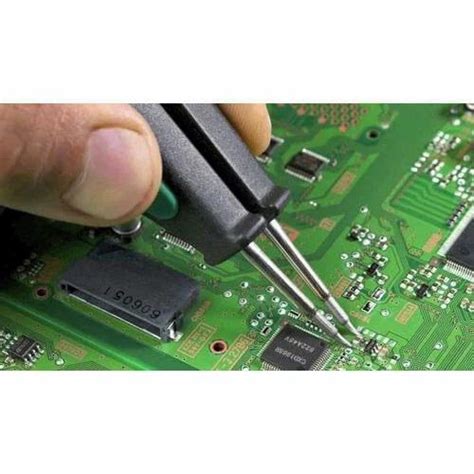
Achieving flawless PCB assembly hinges on mastering precision soldering techniques, which directly impact the functionality and longevity of high-performance electronics. In modern PCBA workflows, soldering accuracy ensures stable electrical connections while minimizing defects like cold joints or bridging. Advanced methods such as surface-mount technology (SMT) and selective soldering enable precise application of solder paste, even for components with pitches below 0.4mm. Temperature-controlled reflow ovens and nitrogen-environments further refine solder joint integrity, particularly for heat-sensitive ICs or fine-pitch BGAs.
Automated optical inspection (AOI) systems complement these processes by detecting micron-level inconsistencies, ensuring alignment with IPC-A-610 standards. For through-hole components, wave soldering remains a cornerstone, balancing speed and uniformity for high-volume production. Critical to success is the interplay between material selection—such as lead-free solder alloys—and equipment calibration, which together mitigate thermal stress and oxidation risks. By integrating these strategies, manufacturers optimize PCB assembly outcomes, delivering boards that meet rigorous performance demands in aerospace, medical, or IoT applications.
Quality Standards in PCB Assembly
Adherence to rigorous quality standards is critical in PCB assembly to ensure the reliability and longevity of electronic devices. Modern PCBA processes align with internationally recognized benchmarks such as IPC-A-610 (Acceptability of Electronic Assemblies) and IPC-J-STD-001 (Requirements for Soldered Electrical Connections). These frameworks define precise criteria for solder joint integrity, component placement accuracy, and material compatibility, minimizing defects like cold joints or tombstoning.
Tip: Always verify that your PCB assembly partner conducts Automated Optical Inspection (AOI) and X-ray testing to detect hidden flaws in high-density boards.
To meet these standards, manufacturers employ controlled environments with stable humidity and temperature, paired with lead-free soldering techniques compliant with RoHS directives. Traceability systems, including barcoding and batch tracking, further enhance quality assurance by documenting each stage of the PCBA workflow. For mission-critical applications, thermal cycling tests and vibration resistance assessments validate performance under extreme conditions.
Transitioning between design and production, designers must collaborate closely with assembly teams to address Design for Manufacturability (DFM) considerations early. This proactive approach reduces rework risks while ensuring alignment with quality benchmarks from prototype to mass production. By integrating these practices, manufacturers achieve consistent outcomes that meet both technical specifications and industry certifications.
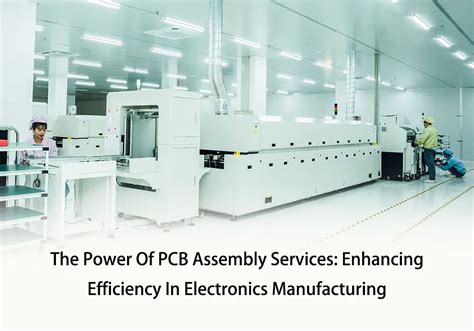
Advanced Equipment for PCB Soldering Success
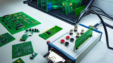
Modern PCB assembly relies heavily on advanced equipment to achieve the precision and repeatability required for high-performance electronics. At the core of PCBA workflows are automated soldering systems, such as selective soldering machines and reflow ovens, which ensure consistent thermal profiles and minimize human error. These systems integrate closed-loop temperature control to maintain optimal conditions for lead-free solder alloys, critical for meeting international safety and durability standards.
For intricate designs, laser-assisted soldering and 3D SPI (Solder Paste Inspection) tools enable micron-level accuracy, detecting voids or misalignments before components are permanently placed. Meanwhile, nitrogen-assisted reflow ovens reduce oxidation during soldering, enhancing joint integrity in high-density boards. Manufacturers leveraging PCB assembly technologies like AOI (Automated Optical Inspection) further streamline quality assurance, identifying defects such as tombstoning or cold joints in real time.
Transitioning to such equipment not only boosts throughput but also aligns with PCBA reliability goals, as tighter process controls reduce rework rates. As electronics shrink in size but grow in complexity, investing in advanced soldering infrastructure becomes indispensable for maintaining competitiveness in industries like aerospace, medical devices, and IoT. This focus on technological precision naturally sets the stage for optimizing soldering parameters—a topic explored in subsequent sections.
Optimizing PCB Soldering for Electronics
Effective PCB assembly relies on precise soldering techniques to ensure electrical reliability and thermal stability in high-performance devices. Achieving optimal results requires balancing temperature control, solder material selection, and equipment calibration. For instance, PCBA processes often employ reflow soldering, where maintaining consistent thermal profiles prevents issues like cold joints or component warping. Advanced systems integrate nitrogen-rich environments to minimize oxidation, enhancing solder joint integrity for dense circuits.
Critical to success is the use of high-quality solder paste with appropriate viscosity and metal composition, matched to the board’s design requirements. Automated stencil printers and pick-and-place machines ensure accuracy, while inline inspection systems, such as automated optical inspection (AOI), validate alignment before soldering. For mixed-technology boards, combining wave soldering for through-hole components with selective soldering for sensitive parts reduces thermal stress.
Engineers must also account for thermal management post-soldering, as uneven heat dissipation can compromise long-term performance. By aligning PCB assembly workflows with industry standards like IPC-A-610, manufacturers achieve repeatable quality while minimizing defects. Partnering with experienced PCBA providers ensures access to cutting-edge techniques, from laser soldering for microcomponents to advanced conformal coating for environmental protection.
Reliability in PCB Assembly Processes
Achieving consistent reliability in PCB assembly requires meticulous attention to both design and execution. At the core of dependable PCBA manufacturing lies the integration of robust material selection, precision-controlled soldering environments, and rigorous testing protocols. For high-performance electronics, even minor deviations in solder joint integrity or component placement can compromise functionality, making adherence to IPC-A-610 and IPC-J-STD-001 standards non-negotiable.
Critical stages such as surface-mount technology (SMT) assembly demand advanced reflow soldering systems to maintain optimal thermal profiles, ensuring uniform melting of solder paste without damaging sensitive components. Concurrently, through-hole assembly processes rely on wave soldering techniques calibrated to avoid cold joints or bridging. To mitigate risks like electrochemical migration or thermal stress, manufacturers employ automated optical inspection (AOI) and X-ray inspection systems, which detect defects invisible to the naked eye.
Furthermore, environmental controls—such as humidity-regulated workspaces and anti-static measures—play a pivotal role in preserving PCB assembly quality. By combining statistical process control (SPC) with real-time data analytics, modern PCBA workflows preemptively address variability, aligning production outcomes with stringent reliability benchmarks. This systematic approach not only minimizes failure rates but also extends the operational lifespan of electronic systems, reinforcing trust in end-product performance.
Best Practices for PCB Assembly
Implementing PCB assembly best practices is critical for achieving consistent quality and reliability in high-performance electronics. A foundational step involves meticulous component selection, ensuring compatibility with design specifications and environmental conditions. During PCBA (Printed Circuit Board Assembly), precise solder paste application using stencil printing techniques minimizes bridging and voids, while automated pick-and-place systems guarantee accurate component positioning.
Adherence to controlled soldering profiles—including temperature gradients and dwell times—prevents thermal stress, a common cause of latent failures. Post-soldering inspections, such as Automated Optical Inspection (AOI) and X-ray analysis, are indispensable for detecting hidden defects like cold joints or micro-cracks. For complex designs, integrating Design for Manufacturability (DFM) principles early in the process reduces rework risks and accelerates production timelines.
Collaboration with certified partners, such as Corintech’s PCB assembly services, ensures access to advanced equipment like reflow ovens with nitrogen environments, which enhance solder joint integrity. Finally, rigorous environmental testing—including thermal cycling and vibration assessments—validates the durability of assembled boards under real-world operating conditions. By aligning these strategies, manufacturers can optimize PCBA outcomes while maintaining compliance with industry standards like IPC-A-610 and ISO 9001.
High-Performance Soldering Solutions
Achieving high-performance soldering in PCB assembly requires a blend of advanced techniques, specialized materials, and meticulous process control. Modern PCBA workflows leverage precision tools like automated solder paste dispensers and nitrogen-reflow ovens to minimize oxidation and ensure consistent joint quality. For applications demanding extreme reliability—such as aerospace or medical devices—low-voiding soldering processes are critical to prevent thermal stress and electrical failures.
The integration of laser soldering and selective soldering systems enables targeted heat application, reducing thermal damage to sensitive components. Additionally, using lead-free solder alloys compliant with RoHS and IPC-A-610 standards ensures environmental safety without compromising conductivity. A growing focus on miniaturization in electronics has also driven adoption of micro-soldering methods, capable of handling components as small as 01005 packages.
To maintain consistency, manufacturers increasingly rely on real-time monitoring systems that track parameters like temperature profiles and solder flow rates. These systems align with the broader shift toward Industry 4.0, where data-driven optimization enhances yield rates. For deeper insights into evolving practices, explore trends in the electronic manufacturing services market. By combining cutting-edge equipment with rigorous quality protocols, PCB assembly providers can deliver soldering solutions that meet the exacting demands of modern high-performance electronics.
Conclusion
In the realm of modern electronics manufacturing, achieving excellence in PCB assembly hinges on harmonizing precision techniques with rigorous adherence to quality standards. As discussed, advanced soldering methods and cutting-edge equipment form the backbone of reliable PCBA outcomes, particularly for high-performance applications. Whether leveraging reflow soldering for surface-mount components or selective soldering for mixed-technology boards, the interplay between process control and material selection remains critical.
To sustain reliability, manufacturers must prioritize thermal management and contamination prevention, aligning with industry benchmarks such as IPC-A-610 and ISO 9001. Partnering with certified providers like Rocket PCB ensures access to expertise in PCB assembly workflows, from prototyping to volume production. As technology evolves, embracing innovations like automated optical inspection (AOI) and AI-driven process optimization will further elevate PCBA consistency. Ultimately, success lies in balancing technical precision with a commitment to continuous improvement—a strategy that safeguards both performance and longevity in an increasingly demanding electronics landscape.
Frequently Asked Questions
What distinguishes PCB assembly from PCBA?
PCB assembly refers to the entire process of populating a bare circuit board with components, while PCBA (Printed Circuit Board Assembly) specifically denotes the completed board after all soldering and testing phases. Both terms are often used interchangeably, but PCBA emphasizes the finalized product ready for integration into electronics.
How do soldering services ensure reliability in high-performance applications?
Advanced PCB assembly providers employ temperature-controlled soldering irons, reflow ovens, and automated optical inspection (AOI) systems. These tools maintain precise thermal profiles and detect micro-defects, ensuring joints withstand mechanical stress and thermal cycling in demanding environments.
What quality standards govern PCB assembly processes?
Leading manufacturers adhere to IPC-A-610 for acceptability criteria and ISO 9001 for process consistency. Compliance with these standards guarantees proper component placement, solder fillet geometry, and electrical continuity—critical for aerospace, medical, or industrial applications.
Can PCBA prototyping accelerate product development?
Yes. Rapid prototyping services enable iterative testing of circuit functionality and layout optimization. By identifying design flaws early, teams reduce time-to-market while maintaining signal integrity and thermal management performance.
How do costs vary between manual and automated soldering services?
Automated PCB assembly excels in high-volume production with uniform quality, while manual soldering suits low-volume or mixed-technology boards. Hybrid approaches balance cost-efficiency for complex designs requiring fine-pitch components or specialized connectors.
Ready to Optimize Your PCB Assembly Workflow?
For tailored PCBA solutions combining precision soldering, rigorous testing, and industry-leading turnaround times, please click here to explore our end-to-end manufacturing capabilities.