The Impact of PCB Design Processes on DFM Technology: Key Specification Requirements
Abstract
Design for Manufacturability (DFM) is a critical aspect of printed circuit board (PCB) development, ensuring that designs are optimized for efficient and cost-effective production. PCB design processes must adhere to specific DFM guidelines to minimize defects, reduce costs, and improve reliability. This paper explores the key DFM requirements imposed by PCB design processes, including material selection, trace routing, component placement, via design, and fabrication constraints. By following these guidelines, designers can enhance manufacturability, reduce production delays, and improve overall product quality.
1. Introduction
The increasing complexity of modern electronics demands rigorous PCB design methodologies that align with DFM principles. DFM ensures that a PCB can be manufactured with minimal errors, high yield, and optimal performance. PCB design processes must consider fabrication, assembly, and testing constraints to meet DFM standards. This paper examines the key DFM requirements influenced by PCB design processes and their impact on manufacturing efficiency.
2. PCB Material Selection and DFM Requirements
2.1 Substrate Material Considerations
The choice of PCB substrate (e.g., FR-4, Rogers, or polyimide) affects thermal performance, signal integrity, and manufacturability. DFM guidelines require:
- Thermal Stability: Materials must withstand reflow soldering temperatures without warping.
- Dielectric Constant: Must be consistent to avoid impedance mismatches in high-frequency designs.
- Layer Stackup: Symmetrical layer stacking prevents warping and improves reliability.
2.2 Copper Weight and Trace Width
- Copper Thickness: Standard 1 oz/ft² copper is preferred for ease of etching; thicker copper requires wider traces to avoid over-etching.
- Trace Width/Spacing: Must comply with fabrication capabilities (e.g., ≥ 4 mil trace/space for standard PCBs).
3. Component Placement and DFM Guidelines
3.1 Optimal Component Layout
- Assembly Efficiency: Components should be placed to minimize soldering defects (e.g., tombstoning in SMT parts).
- Thermal Management: High-power components must be spaced appropriately to avoid overheating.
- Testability: Adequate spacing for probe access in automated testing.
3.2 Footprint Design Standards
- Land Patterns: Must match component datasheets to prevent misalignment.
- Solder Mask Clearance: Prevents solder bridging while ensuring proper solder wetting.
4. Trace Routing and Signal Integrity
4.1 Impedance Control
- Controlled impedance traces (e.g., 50Ω for RF circuits) require precise width and dielectric spacing.
- Differential pairs must maintain consistent spacing to minimize skew.
4.2 High-Speed Design Constraints
- Length Matching: Critical for high-speed signals (e.g., DDR, PCIe).
- Via Stub Minimization: Back-drilling or blind vias reduce signal reflections.
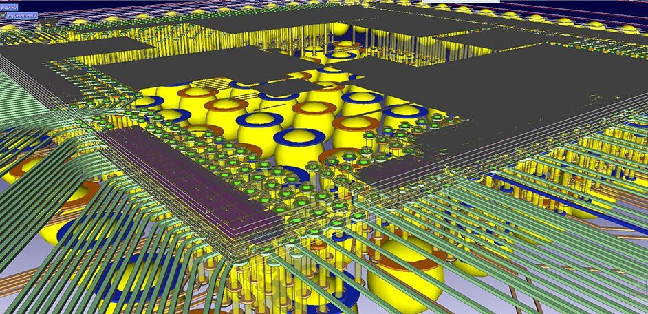
5. Via Design and DFM Compliance
5.1 Via Types and Applications
- Through-Hole Vias: Standard for low-cost designs but consume more space.
- Blind/Buried Vias: Used in HDI designs but increase fabrication complexity.
- Microvias: Essential for high-density interconnects but require laser drilling.
5.2 Via Reliability Considerations
- Aspect Ratio: Should not exceed manufacturer limits (typically 8:1 for through-hole vias).
- Via-in-Pad: Requires filling and plating to prevent solder wicking.
6. Solder Mask and Silkscreen Requirements
6.1 Solder Mask Application
- Clearance: Must expose pads adequately while preventing solder bridging.
- Registration Tolerance: Misalignment can lead to exposed copper or blocked pads.
6.2 Silkscreen Legibility
- Text Size: Minimum 0.8mm height for readability.
- Avoiding Critical Areas: Should not overlap pads or vias.
7. Panelization and Fabrication Efficiency
7.1 Panel Design for Mass Production
- Breakaway Tabs: Must allow easy depanelization without damaging boards.
- Fiducial Marks: Essential for automated assembly alignment.
7.2 Tooling Holes and Fiducials
- Standardized tooling holes ensure proper alignment during fabrication and assembly.
8. Testing and Inspection Compliance
8.1 Design for Test (DFT) Requirements
- Test Points: Must be accessible for in-circuit testing (ICT).
- Boundary Scan: JTAG compliance for complex digital boards.
8.2 Automated Optical Inspection (AOI) Considerations
- Component Contrast: High contrast between parts and PCB aids inspection.
- Avoiding Shadowing: Tall components should not obscure smaller ones.
9. Conclusion
PCB design processes must adhere to strict DFM guidelines to ensure manufacturability, reliability, and cost efficiency. Key considerations include material selection, component placement, trace routing, via design, solder mask application, and panelization strategies. By integrating DFM principles early in the design phase, engineers can minimize production issues, reduce costs, and accelerate time-to-market. Future advancements in PCB technology, such as flexible and high-density interconnects, will further refine DFM requirements, necessitating continuous adaptation in design practices.