Causes of PCB Pad Lifting and Poor Solderability: A Comprehensive Analysis
Introduction
Printed Circuit Board (PCB) reliability is critical in electronics manufacturing, and among the most common issues encountered are pad lifting (pad detachment) and poor solderability (difficulty in achieving proper solder wetting). These problems can lead to catastrophic failures, increased production costs, and significant quality control challenges. This 2000-word article examines the root causes of these issues, covering material factors, manufacturing processes, design considerations, and environmental influences that contribute to pad lifting and poor solderability in PCB assembly.
Section 1: Understanding PCB Pad Lifting
1.1 Definition and Manifestations
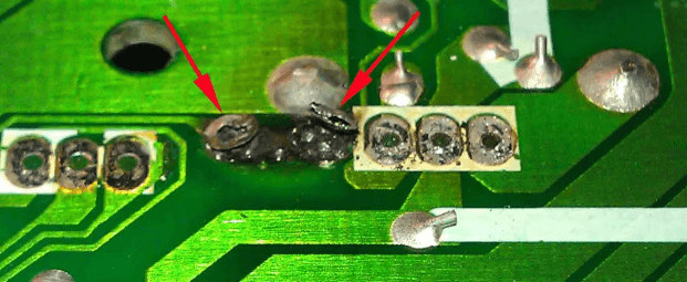
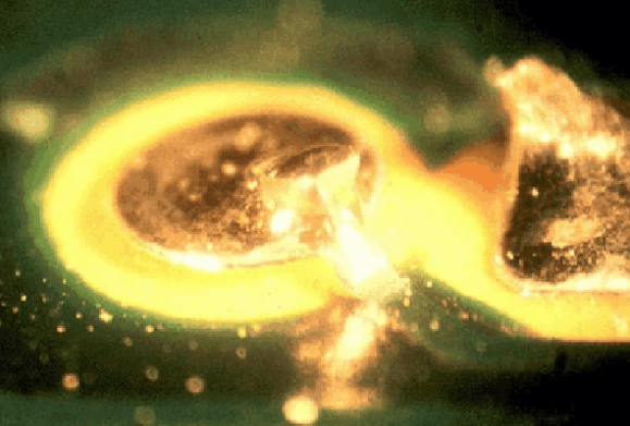
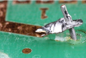
Pad lifting refers to the partial or complete detachment of copper pads from the PCB substrate, which can occur during soldering, rework, or even in normal operation. This phenomenon manifests as:
- Visible separation between pad and substrate
- Cracking sounds during thermal cycling
- Complete pad detachment during component replacement
- Intermittent electrical connections
1.2 Primary Causes of Pad Lifting
1.2.1 Thermal Stress and CTE Mismatch
The coefficient of thermal expansion (CTE) mismatch between copper (≈17 ppm/°C) and common FR-4 substrate (≈13-15 ppm/°C in x-y, ≈50-70 ppm/°C in z-axis) creates mechanical stress during temperature variations. During soldering (typically 220-260°C), this mismatch can exceed the adhesive strength of the copper-to-substrate bond.
1.2.2 Poor Copper Adhesion
Inadequate bonding between copper and substrate results from:
- Improper surface preparation during PCB fabrication
- Contamination on the dielectric surface
- Insufficient oxide treatment for inner layers
- Low-quality laminate materials
1.2.3 Excessive Mechanical Stress
Physical forces contribute to pad lifting through:
- Overuse of mechanical force during hand soldering
- Excessive vacuum pickup pressure during automated assembly
- Improper use of tweezers or tools during rework
- Board flexure during handling or in final application
1.2.4 Multiple Rework Cycles
Each rework operation subjects pads to:
- Additional thermal cycles that degrade adhesion
- Mechanical stress from component removal
- Potential localized overheating
- Chemical exposure from flux residues
1.2.5 Design-Related Factors
Poor design practices that promote pad lifting include:
- Insufficient annular ring around vias
- Pads with minimal copper anchors
- High aspect ratio plated through holes
- Pads connected to large copper areas without thermal relief
Section 2: Causes of Poor Solderability
2.1 Definition and Symptoms
Poor solderability refers to the inability of molten solder to properly wet and adhere to PCB pads, characterized by:
- Solder beading up rather than spreading evenly
- Dull, grainy solder joints instead of shiny surfaces
- Incomplete fillet formation
- Excessive voiding in solder joints
2.2 Primary Causes of Poor Solderability
2.2.1 Surface Oxidation
Copper readily forms oxides that impair solderability:
- Exposure to air forms Cu₂O (cuprous oxide) and CuO (cupric oxide)
- High humidity accelerates oxidation
- Elevated temperatures during storage increase oxide growth
- Sulfur-containing environments create non-solderable copper sulfide
2.2.2 Contamination
Various contaminants prevent proper solder wetting:
- Finger oils from handling
- Flux residues from previous processes
- Silicone contamination from molds or release agents
- Dust and particulate matter accumulation
- Chemical residues from cleaning processes
2.2.3 Improper Surface Finishes
Common PCB finishes and their solderability challenges:
- HASL (Hot Air Solder Leveling): Thick, uneven surfaces; tin-lead depletion
- ENIG (Electroless Nickel Immersion Gold): Black pad syndrome; nickel oxidation
- Immersion Silver: Tarnishing; creep corrosion
- OSP (Organic Solderability Preservative): Degradation over time; thermal decomposition
2.2.4 Inadequate Flux Activity
Flux-related issues include:
- Insufficient flux quantity or coverage
- Wrong flux type for the application (RA vs. RMA vs. no-clean)
- Expired or degraded flux materials
- Incompatibility with solder alloy
2.2.5 Soldering Process Parameters
Improper process settings affecting solderability:
- Temperature too low for proper wetting
- Excessive temperature causing flux burnout
- Insufficient time above liquidus
- Incorrect soldering atmosphere (oxygen content in reflow)
Section 3: Combined Factors Affecting Both Pad Lifting and Solderability
3.1 PCB Fabrication Issues
Manufacturing defects that impact both pad integrity and solderability:
- Incomplete etching leaving copper residues
- Over-etching reducing pad thickness
- Poor plating quality in through-holes
- Lamination voids under pads
- Improper cure of solder mask adjacent to pads
3.2 Material Selection Problems
Inappropriate material choices contributing to both issues:
- Low-Tg laminates for high-temperature applications
- Thin copper foils for heavy components
- Incompatible combinations of surface finishes and solders
- Low-quality base materials with impurities
3.3 Storage and Handling Conditions
Environmental factors during storage:
- Excessive humidity (>60% RH) promoting oxidation
- High temperatures accelerating material degradation
- Exposure to corrosive atmospheres (H₂S, Cl₂, etc.)
- Extended storage beyond material shelf life
- Improper packaging allowing moisture ingress
3.4 Process Incompatibilities
Conflicts between materials and processes:
- Lead-free solders requiring higher temperatures than finish can withstand
- Mixed metallurgy creating intermetallic issues
- Cleaning processes that damage surfaces
- Multiple thermal excursions degrading materials
Section 4: Prevention and Mitigation Strategies
4.1 Design for Reliability
- Implement proper thermal relief connections
- Ensure adequate annular rings for vias
- Balance copper distribution for even heating
- Specify appropriate materials for the application
- Consider mechanical stress points in layout
4.2 Manufacturing Controls
- Strict process controls in PCB fabrication
- Comprehensive cleanliness protocols
- Proper handling to prevent contamination
- Controlled application of surface finishes
- Rigorous quality inspection of incoming boards
4.3 Storage and Handling Best Practices
- Maintain controlled environment (25°C, <40% RH ideal)
- Use moisture barrier bags with desiccant for sensitive finishes
- Implement first-in-first-out inventory management
- Limit board exposure prior to assembly
- Follow manufacturer’s shelf life recommendations
4.4 Process Optimization
- Profile soldering processes for each board type
- Match flux chemistry to application requirements
- Control rework thermal profiles and techniques
- Implement nitrogen atmospheres where beneficial
- Establish proper cleaning procedures when needed
Conclusion
PCB pad lifting and poor solderability stem from complex interactions between materials, design, manufacturing processes, and environmental factors. Thermal and mechanical stresses, surface contamination, oxidation, and improper material selection represent the primary root causes. Addressing these issues requires a holistic approach encompassing thoughtful design, controlled manufacturing, proper handling, and optimized assembly processes. By understanding these underlying causes, electronics manufacturers can implement targeted prevention strategies to improve product reliability and manufacturing yield. Continuous attention to these factors becomes increasingly critical as PCB technology advances toward finer pitches, higher densities, and more demanding applications.