Preventing PCB Damage: Essential Guidelines for Longevity and Reliability
Printed Circuit Boards (PCBs) are the backbone of modern electronics, serving as the foundation for everything from consumer gadgets to industrial machinery. However, PCBs are susceptible to various types of damage, including mechanical stress, electrical overload, thermal issues, and environmental factors. Preventing PCB damage is crucial for ensuring device reliability, reducing repair costs, and extending product lifespan. This article provides a comprehensive guide on avoiding PCB damage, covering design, manufacturing, handling, and operational best practices.
1. Proper PCB Design Considerations
A well-designed PCB is less prone to failure. Key design aspects to consider include:
A. Optimal Trace Layout and Width
- Ensure traces are wide enough to handle the expected current without overheating.
- Avoid sharp angles in traces, as they can cause signal integrity issues and increase electromagnetic interference (EMI).
- Use proper spacing between traces to prevent short circuits and crosstalk.
B. Thermal Management
- Incorporate thermal relief pads for components that generate heat.
- Use copper pours and heat sinks to dissipate heat efficiently.
- Place temperature-sensitive components away from high-heat areas.
C. Component Placement and Routing
- Position high-power components strategically to avoid localized overheating.
- Minimize long signal paths to reduce impedance and signal degradation.
- Follow manufacturer-recommended footprints for components to ensure proper soldering.
D. Protection Circuits
- Implement fuses, transient voltage suppressors (TVS), and ESD protection diodes to guard against power surges and electrostatic discharge.
- Use current-limiting resistors to prevent overloading sensitive components.
2. Careful Manufacturing and Assembly Practices
Even the best-designed PCB can fail if manufacturing and assembly are flawed. Follow these guidelines:
A. Quality Materials and Fabrication
- Use high-quality substrates (e.g., FR-4 for general applications, high-Tg materials for high-temperature environments).
- Ensure proper copper thickness based on current requirements.
- Verify that the PCB manufacturer follows IPC standards for fabrication.
B. Soldering Best Practices
- Avoid cold solder joints by maintaining proper temperature profiles during reflow or wave soldering.
- Use lead-free solder where environmental regulations apply, but ensure compatibility with components.
- Apply solder mask to prevent unintended bridging between pads.
C. Inspection and Testing
- Conduct Automated Optical Inspection (AOI) to detect soldering defects.
- Perform In-Circuit Testing (ICT) and functional testing to verify electrical performance.
- Use X-ray inspection for hidden defects in multilayer PCBs or BGAs.
3. Safe Handling and Storage Procedures
Improper handling is a leading cause of PCB damage. Follow these precautions:
A. Anti-Static Measures
- Always handle PCBs in an Electrostatic Discharge (ESD)-safe environment.
- Use grounded wrist straps, anti-static mats, and ESD-safe containers.
- Avoid touching exposed traces or connectors with bare hands.
B. Mechanical Protection
- Store PCBs in protective trays or anti-static bags to prevent bending or scratching.
- Avoid stacking PCBs unless separated by foam or spacers.
- Use proper tools (e.g., non-metallic tweezers) during assembly to prevent physical damage.
C. Environmental Controls
- Store PCBs in a dry, temperature-controlled environment to prevent moisture absorption (which can lead to delamination or “popcorning” during reflow).
- If exposed to humidity, bake the PCBs before soldering to remove moisture.

4. Preventing Electrical Damage During Operation
Even after successful manufacturing and assembly, PCBs can fail due to electrical issues. Mitigate risks with these strategies:
A. Overvoltage and Overcurrent Protection
- Use voltage regulators and fuses to prevent excessive voltage or current.
- Incorporate reverse polarity protection diodes to avoid damage from incorrect power connections.
- Employ resettable fuses (PTCs) for self-recovering overcurrent protection.
B. EMI and Noise Reduction
- Implement proper grounding techniques (star grounding for analog circuits, ground planes for digital circuits).
- Use decoupling capacitors near ICs to filter high-frequency noise.
- Shield sensitive circuits with grounded metal enclosures if necessary.
C. Avoiding Short Circuits
- Inspect for stray conductive debris (e.g., solder balls, metal shavings) before powering up.
- Ensure no exposed traces or component leads are touching unintended conductors.
5. Thermal Management Strategies
Excessive heat is a major cause of PCB failure. Prevent thermal damage with these methods:
A. Proper Ventilation and Cooling
- Use fans, heat sinks, or thermal vias to dissipate heat.
- Ensure adequate airflow in enclosed systems.
- Avoid placing heat-sensitive components near high-power devices.
B. Thermal Cycling Considerations
- Use flexible PCBs or strain relief for applications with frequent temperature changes.
- Select components with appropriate temperature ratings for the operating environment.
C. Monitoring and Alerts
- Integrate temperature sensors to trigger cooling systems or shutdowns in case of overheating.
- Log thermal data to identify potential failure points before they cause damage.
6. Environmental and Chemical Protection
PCBs exposed to harsh environments require additional safeguards:
A. Conformal Coating
- Apply acrylic, silicone, or polyurethane coatings to protect against moisture, dust, and chemicals.
- Ensure coatings are compatible with component tolerances and rework requirements.
B. Enclosure Design
- Use IP-rated enclosures for water and dust resistance.
- Seal connectors and openings to prevent corrosive gas or liquid ingress.
C. Avoiding Chemical Exposure
- Keep PCBs away from solvents, acids, and other corrosive substances.
- Clean PCBs with isopropyl alcohol (IPA) rather than harsh chemicals.
7. Regular Maintenance and Inspection
Proactive maintenance can prevent unexpected failures:
A. Visual Inspections
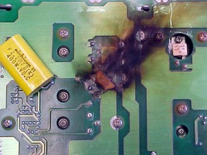
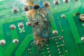
- Look for signs of corrosion, burnt components, or cracked solder joints.
- Check for bulging or leaking capacitors.
B. Performance Testing
- Periodically test power delivery, signal integrity, and thermal performance.
- Use thermal imaging to detect hotspots before they cause failures.
C. Firmware and Software Updates
- Ensure embedded systems have up-to-date firmware to prevent software-induced hardware issues (e.g., overclocking, incorrect PWM settings).
Conclusion
Preventing PCB damage requires a holistic approach, encompassing design, manufacturing, handling, operation, and maintenance. By following these best practices, engineers and technicians can significantly reduce the risk of PCB failure, ensuring long-term reliability and performance. Investing in proper design, quality materials, and protective measures ultimately saves time, money, and frustration while extending the lifespan of electronic devices.
By adhering to these guidelines, manufacturers and end-users alike can minimize PCB-related failures and maximize the efficiency and durability of their electronic systems.