The Concept and Role of PCB Symbols in Electronic Design
Introduction
Printed Circuit Boards (PCBs) are the backbone of modern electronics, providing mechanical support and electrical connections for electronic components. A crucial aspect of PCB design is the use of PCB symbols, which serve as graphical representations of electronic components in schematic diagrams. Understanding PCB symbols is essential for engineers, designers, and hobbyists involved in electronics development. This article explores the concept of PCB symbols, their types, standardization, and their critical role in PCB design.
1. What Are PCB Symbols?
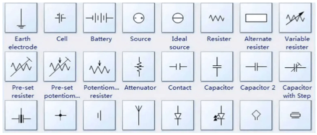
PCB symbols, also known as schematic symbols, are standardized graphical representations of electronic components used in circuit schematics. These symbols abstract the physical appearance of components, focusing instead on their electrical functionality.
Key Characteristics of PCB Symbols:
- Graphical Representation: Each symbol visually depicts a component (e.g., resistors, capacitors, ICs).
- Electrical Functionality: Symbols indicate how components interact in a circuit.
- Standardization: Most symbols follow industry standards (e.g., IEEE, IEC, ANSI).
- Connection Points (Pins): Symbols include designated pins that correspond to physical component leads.
For example:
- A resistor is represented by a zigzag line (IEEE standard) or a rectangle (IEC standard).
- A capacitor is shown as two parallel lines (for non-polarized) or a curved line with a straight line (for polarized).
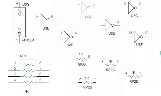
- An integrated circuit (IC) is depicted as a rectangle with labeled pins.
2. Types of PCB Symbols
PCB symbols can be categorized based on component types and their roles in circuit design.
2.1 Passive Components
These components do not require external power and include:
- Resistors (fixed, variable, thermistors)
- Capacitors (ceramic, electrolytic, film)
- Inductors (coils, transformers)
2.2 Active Components
These components rely on an external power source and include:
- Diodes (standard, Zener, LEDs)
- Transistors (BJT, MOSFET)
- Integrated Circuits (ICs) (microcontrollers, op-amps)
2.3 Electromechanical Components
These involve mechanical and electrical interactions:
- Switches (toggle, push-button)
- Relays
- Connectors (headers, USB ports)
2.4 Power Sources
- Batteries
- Voltage sources (DC/AC)
3. The Role of PCB Symbols in Circuit Design
PCB symbols play several critical roles in electronics design:
3.1 Schematic Capture
Before designing a PCB layout, engineers create a schematic diagram using PCB symbols. This diagram serves as a blueprint, illustrating:
- Component connections
- Power and ground distribution
- Signal flow
3.2 Standardization and Clarity
Standardized symbols ensure that schematics are universally understood, reducing errors in interpretation. For example:
- A triangle represents an operational amplifier (op-amp).
- A zigzag line always denotes a resistor (in IEEE standards).
3.3 Linking Schematics to PCB Layouts
PCB symbols are associated with footprints (physical layouts) in PCB design software (e.g., Altium Designer, KiCad). This linkage ensures that:
- Each symbol corresponds to a real-world component.
- Pin assignments match between schematic and PCB layout.
3.4 Error Detection and Troubleshooting
A well-drawn schematic with correct symbols helps in:
- Identifying incorrect connections.
- Detecting missing power or ground connections.
- Simplifying debugging during prototyping.
3.5 Collaboration Among Engineers
Since PCB symbols follow industry standards, they facilitate seamless collaboration between:
- Hardware designers
- PCB layout engineers
- Manufacturers
4. PCB Symbol Standards
Different organizations have established standards for PCB symbols to ensure consistency.
4.1 IEEE/ANSI Standards (US)
- Uses zigzag lines for resistors.
- Employs rectangular shapes for logic gates.
4.2 IEC Standards (International)
- Prefers rectangular resistors.
- Uses simplified logic gate symbols.
4.3 Differences Between Standards
| Component | IEEE/ANSI Symbol | IEC Symbol |
|---|---|---|
| Resistor | Zigzag line | Rectangle |
| Capacitor | Parallel lines | Parallel lines (similar) |
| Diode | Triangle with line | Triangle with line (similar) |
Engineers must adhere to the appropriate standard based on regional or company requirements.
5. Creating and Managing PCB Symbols
Modern PCB design tools allow engineers to create and manage custom symbols.
5.1 Steps to Create a PCB Symbol
- Define the Component: Determine electrical properties (e.g., pin count, polarity).
- Draw the Symbol: Use a schematic editor to design the graphical representation.
- Assign Pins: Label each pin with its function (e.g., VCC, GND, input/output).
- Link to Footprint: Associate the symbol with a physical PCB footprint.
5.2 Best Practices for PCB Symbol Design
- Consistency: Follow the same style (IEEE or IEC) throughout the schematic.
- Clear Labeling: Ensure pin names and reference designators (e.g., R1, C2) are readable.
- Avoid Overlapping: Prevent symbol overlaps to maintain clarity.
6. Common Mistakes in PCB Symbol Usage
- Incorrect Pin Assignments: Misplaced VCC/GND pins can cause circuit failure.
- Non-Standard Symbols: Using custom symbols without documentation can confuse collaborators.
- Missing Power Connections: Forgetting to include power pins in IC symbols.
7. Conclusion
PCB symbols are fundamental to electronic design, serving as the bridge between conceptual schematics and physical PCB layouts. By adhering to standardized symbols, engineers ensure accuracy, efficiency, and collaboration in PCB development. Whether designing a simple circuit or a complex motherboard, understanding and correctly using PCB symbols is essential for successful electronics manufacturing.
As PCB technology evolves, symbol libraries and design tools continue to improve, further streamlining the process of turning ideas into functional electronic devices.