Safety Spacing in PCB Design: A Comprehensive Guide
1. Introduction
Printed Circuit Board (PCB) design is a critical aspect of electronic product development, influencing performance, reliability, and manufacturability. One of the most important considerations in PCB layout is safety spacing, which refers to the minimum allowable distance between conductive elements to prevent electrical, thermal, and mechanical failures. Proper spacing ensures signal integrity, reduces crosstalk, prevents short circuits, and enhances manufacturability.
This article explores the key aspects of safety spacing in PCB design, including:
- Electrical Spacing (voltage isolation, creepage, and clearance)
- Signal Integrity Spacing (impedance control, crosstalk avoidance)
- Manufacturing Spacing (fabrication tolerances, solder mask requirements)
- Thermal Spacing (heat dissipation, high-current traces)
- Component Placement Spacing (assembly and rework considerations)
By understanding and implementing proper safety spacing, designers can optimize PCB performance while minimizing risks.
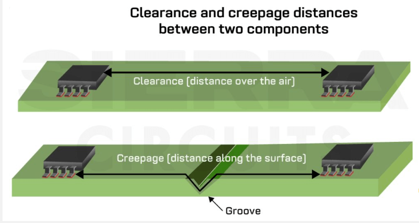
2. Electrical Spacing: Clearance and Creepage
2.1 Clearance (Air Gap)
Clearance refers to the shortest distance between two conductive elements through air. It is crucial for preventing arcing and electrical breakdown, especially in high-voltage applications.
- Low-Voltage PCBs (≤ 30V): Typically require 0.1mm to 0.2mm clearance.
- Medium-Voltage (30V–150V): Requires 0.5mm to 1mm.
- High-Voltage (≥ 150V): Follow standards like IPC-2221 or IEC 60950, which may require 2mm or more.
2.2 Creepage (Surface Distance)
Creepage is the shortest path between conductors along the surface of the PCB. It prevents leakage currents and tracking (degradation due to contaminants).
- Standard PCBs: Typically 0.25mm–0.5mm.
- High-Humidity or Polluted Environments: Requires larger creepage (up to 2x clearance).
2.3 IPC and IEC Standards
- IPC-2221: General guidelines for PCB spacing.
- IEC 60664: Insulation coordination for electrical equipment.
- UL/EN Safety Standards: Mandatory for consumer and industrial electronics.
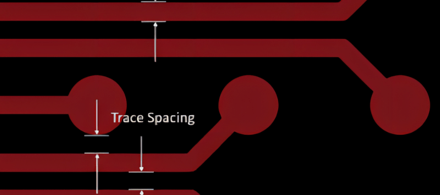
3. Signal Integrity Spacing
3.1 Trace-to-Trace Spacing
To minimize crosstalk and electromagnetic interference (EMI), traces should maintain proper spacing:
- Digital Signals: At least 3x trace width (e.g., 0.3mm for a 0.1mm trace).
- High-Speed Signals (DDR, USB, HDMI): Follow 3W rule (3x width) or differential pair spacing guidelines.
3.2 Impedance Control
Controlled impedance traces (e.g., 50Ω for RF, 90Ω for USB) require precise spacing:
- Microstrip Lines: Spacing between signal and ground plane affects impedance.
- Stripline Designs: Requires symmetrical spacing between reference planes.
3.3 High-Frequency Considerations
- Avoid Parallel Long Traces: Reduces inductive coupling.
- Ground Guard Traces: Isolate sensitive signals with grounded traces.
4. Manufacturing Spacing (DFM Considerations)
4.1 Minimum Trace/Space Requirements
PCB manufacturers specify minimum tolerances:
- Standard Fab: 0.1mm trace/space.
- Advanced Fab (HDI): 0.05mm or less (laser-drilled microvias).
4.2 Solder Mask and Silkscreen Spacing
- Solder Mask Clearance: 0.05mm–0.1mm beyond pads to prevent bridging.
- Silkscreen Text: Should not overlap pads or vias (≥ 0.2mm clearance).
4.3 Via and Hole Spacing
- Drill-to-Copper: ≥ 0.2mm to avoid breakout.
- Via-to-Via Spacing: ≥ 0.3mm for mechanical reliability.
5. Thermal Spacing (High-Current and Heat Dissipation)
5.1 High-Current Traces
- Wider Traces: Reduce resistance (e.g., 1mm width per 1A current).
- Spacing for Heat Dissipation: ≥ 1mm between high-power components.
5.2 Thermal Relief Pads
- Prevent Heat Sinking: Use thermal spokes in pads for easier soldering.
6. Component Placement Spacing
6.1 Assembly and Rework
- Component-to-Component: ≥ 0.5mm for hand soldering, ≥ 0.3mm for automated assembly.
- Edge Clearance: ≥ 1mm from PCB edges to avoid cracking.
6.2 Test Points and Probes
- Probe Spacing: ≥ 1mm for bed-of-nails testing.
7. Common Mistakes and Best Practices
7.1 Common Errors
- Insufficient High-Voltage Spacing: Leads to arcing.
- Ignoring Creepage in Humid Environments: Causes leakage.
- Overlooking Manufacturing Limits: Causes fabrication issues.
7.2 Best Practices
- Use Design Rule Checks (DRC): Automate spacing validation.
- Follow IPC Standards: Ensures reliability.
- Simulate Critical Signals: Verify crosstalk and EMI.
8. Conclusion
Safety spacing in PCB design is a multidimensional challenge, balancing electrical safety, signal integrity, manufacturability, and thermal management. By adhering to industry standards (IPC, IEC) and leveraging modern design tools, engineers can optimize PCB layouts for performance and reliability. Proper spacing not only prevents failures but also reduces costs by minimizing rework and improving yield.