Effective Methods to Reduce Design Risks in PCB Design
Introduction
Printed Circuit Board (PCB) design is a critical phase in electronic product development, where even minor errors can lead to significant manufacturing defects, performance issues, or costly redesigns. As PCBs become more complex with high-speed signals, dense layouts, and advanced materials, the risk of design failures increases. To mitigate these risks, engineers must adopt best practices that enhance reliability, manufacturability, and functionality. This article explores effective methods to reduce design risks in PCB development, covering schematic design, layout optimization, signal integrity, thermal management, and design validation.
1. Comprehensive Schematic Design Review
A well-structured schematic is the foundation of a reliable PCB. Errors at this stage can propagate into the layout, leading to functional failures.
Key Practices:
- Component Selection & Verification:
- Use verified components with available datasheets and footprints.
- Cross-check pin assignments, power requirements, and tolerances.
- Hierarchical Design:
- Break the schematic into functional blocks for better readability and error detection.
- Design Rule Checks (DRC):
- Run automated DRC tools to detect unconnected nets, duplicate components, or incorrect values.
- Peer Review:
- Conduct manual reviews with team members to catch logical errors that automated tools may miss.
2. Optimizing PCB Layout for Manufacturability
A poorly designed layout can cause signal integrity issues, EMI problems, and manufacturing defects.
Key Practices:
- Follow DFM (Design for Manufacturability) Guidelines:
- Adhere to manufacturer-specific constraints (trace width, spacing, via sizes).
- Avoid acute angles in traces to prevent etching issues.
- Layer Stackup Planning:
- Use a symmetrical stackup to prevent warping.
- Assign power and ground planes properly to minimize noise.
- Component Placement Strategy:
- Group related components to minimize trace lengths.
- Place critical components (oscillators, high-speed ICs) first.
- Thermal Management:
- Distribute heat-generating components evenly.
- Use thermal vias and copper pours for heat dissipation.
3. Ensuring Signal Integrity in High-Speed Designs
High-speed signals are prone to reflections, crosstalk, and timing issues.
Key Practices:
- Impedance Control:
- Match trace impedance to the transmission line requirements (e.g., 50Ω for single-ended, 100Ω for differential pairs).
- Use controlled dielectric materials for consistent impedance.
- Proper Routing Techniques:
- Route high-speed signals (clocks, USB, HDMI) with minimal bends and avoid crossing split planes.
- Use differential pairs with tight coupling to reduce EMI.
- Minimize Crosstalk:
- Increase spacing between parallel traces (>3x trace width).
- Use ground guards between sensitive signals.
- Termination Strategies:
- Apply series or parallel termination to reduce reflections in high-speed lines.
4. Power Integrity and Noise Reduction
Power distribution issues can lead to voltage drops, noise, and unstable operation.
Key Practices:
- Decoupling Capacitor Placement:
- Place decoupling capacitors close to IC power pins.
- Use a mix of bulk (10μF) and high-frequency (0.1μF) capacitors.
- Power Plane Design:
- Use solid power and ground planes to reduce impedance.
- Avoid splitting planes under high-speed signals.
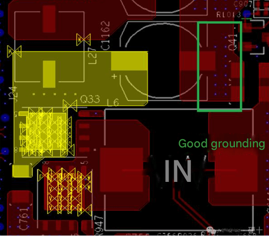
- Minimize Ground Loops:
- Use a single-point ground for analog and digital sections.
- Implement star grounding in mixed-signal designs.
5. Thermal Management Strategies
Overheating reduces component lifespan and can cause intermittent failures.
Key Practices:
- Thermal Analysis:
- Use simulation tools (e.g., Ansys, Cadence Celsius) to identify hotspots.
- Heat Dissipation Techniques:
- Use thermal vias under high-power components.
- Add heatsinks or fans if necessary.
- Copper Pour Utilization:
- Increase copper area for better heat spreading.
6. Design Validation and Testing
Thorough verification prevents costly post-production failures.
Key Practices:
- Design Rule Checking (DRC) & Electrical Rule Checking (ERC):
- Run automated checks before finalizing the layout.
- Signal Integrity Simulation:
- Use tools like HyperLynx or Sigrity to analyze signal quality.
- Prototype Testing:
- Test prototypes under real-world conditions (temperature, vibration, EMI).
- Design for Testability (DFT):
- Include test points for critical signals.
- Use boundary scan (JTAG) for complex boards.
7. Documentation and Version Control
Poor documentation can lead to assembly errors and miscommunication.
Key Practices:
- Maintain Clear Documentation:
- Provide assembly drawings, BOM (Bill of Materials), and fabrication notes.
- Version Control:
- Use Git or SVN to track design revisions.
- Label each revision with changes made.
Conclusion
Reducing design risks in PCB development requires a systematic approach, from schematic design to final validation. By implementing robust design practices—such as thorough schematic reviews, optimized layouts, signal integrity management, and rigorous testing—engineers can minimize errors, improve manufacturability, and enhance product reliability. As PCB technology evolves, staying updated with industry standards and simulation tools will further mitigate risks and ensure successful designs.
By adopting these best practices, design teams can significantly lower the chances of costly re-spins, delays, and field failures, ultimately delivering high-quality PCBs that meet performance and reliability expectations.