How to Create a Complete PCB Engineering Project and Output Documentation
Introduction
Printed Circuit Board (PCB) design is a complex process that requires careful planning, execution, and documentation. A complete PCB engineering project involves multiple stages from concept to manufacturing, with proper documentation being critical at each step. This 2000-word guide will walk you through the entire process of creating a PCB project and generating all necessary output documentation for successful manufacturing and assembly.
1. Project Planning and Requirements Analysis
1.1 Defining Project Specifications
Before starting any PCB design, clearly define:
- The board’s purpose and functionality
- Performance requirements
- Operating environment (temperature, humidity, vibration)
- Power requirements
- Size constraints
- Regulatory compliance needs (FCC, CE, etc.)
- Expected production volume
1.2 Creating a Project Plan
Develop a comprehensive plan that includes:
- Project timeline with milestones
- Resource allocation
- Risk assessment
- Budget considerations
- Verification and testing strategy
Document these specifications in a Project Requirements Document (PRD) that will guide the entire development process.
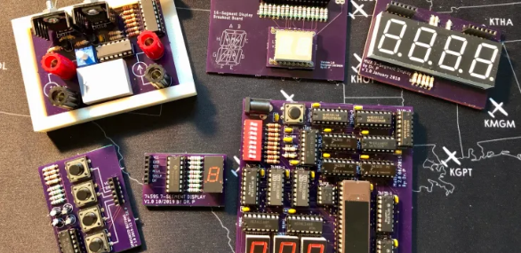
2. Schematic Design
2.1 Component Selection
Choose components based on:
- Functional requirements
- Availability and lead times
- Cost considerations
- Package types
- Thermal characteristics
Create a component database that includes:
- Manufacturer part numbers
- Datasheets
- Footprint information
- Alternative parts
2.2 Schematic Capture
Using EDA (Electronic Design Automation) software:
- Create a new schematic project
- Place all components
- Make electrical connections
- Add power and ground nets
- Include test points for debugging
- Add notes and design constraints
2.3 Schematic Verification
Perform these checks:
- Electrical Rules Check (ERC)
- Connectivity verification
- Power network analysis
- Signal integrity preliminary analysis
- Design rule validation
Generate a Schematic Review Report that documents any issues found and their resolutions.
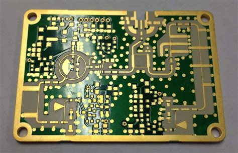
3. PCB Layout Design
3.1 Board Outline Definition
Define the physical board characteristics:
- Board shape and dimensions
- Layer stackup (number of layers, materials, thickness)
- Keep-out areas
- Mounting hole locations
- Connector placement constraints
3.2 Component Placement
Follow these guidelines:
- Place connectors and mechanical components first
- Position critical components (processors, memory, etc.)
- Arrange supporting circuitry
- Consider thermal management
- Optimize for signal integrity
- Document placement rationale in a Placement Report
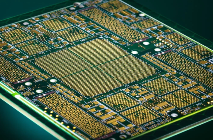
3.3 Routing
Implement proper routing techniques:
- Route critical signals first (clocks, high-speed, sensitive analog)
- Follow impedance control requirements
- Maintain proper clearance and creepage distances
- Implement power distribution network
- Use appropriate via types and sizes
- Document any special routing considerations
3.4 Design Verification
Perform comprehensive checks:
- Design Rule Check (DRC)
- Electrical Rule Check (ERC)
- Signal integrity analysis
- Power integrity analysis
- Thermal analysis
- Manufacturability analysis (DFM)
- Testability analysis (DFT)
Generate a Design Verification Report summarizing findings and any design modifications made.
4. Output Documentation Generation
4.1 Manufacturing Files
Generate these essential files for fabrication:
- Gerber Files (RS-274X format):
- Copper layers (.GTL, .GBL, etc.)
- Solder mask (.GTS, .GBS)
- Silkscreen (.GTO, .GBO)
- Drill drawing (.GDG)
- Board outline (.GKO or .GM1)
- NC Drill Files:
- Excellon format drill file (.TXT)
- Drill map or drawing
- IPC-356 Netlist for bare board testing
- ODB++ or IPC-2581 files (alternative to Gerbers)
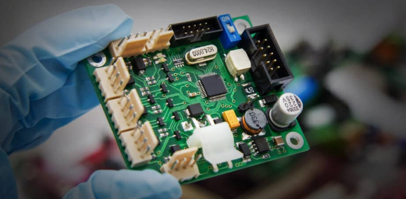
4.2 Assembly Files
Generate these files for component assembly:
- Bill of Materials (BOM) including:
- Reference designators
- Manufacturer part numbers
- Descriptions
- Quantities
- Footprint information
- Alternative parts
- Pick and Place File containing:
- Component reference designators
- X-Y coordinates
- Rotation angles
- Side of board (top/bottom)
- Assembly Drawings showing:
- Component locations
- Orientation indicators
- Special assembly instructions
- Reference designators
4.3 Testing Documentation
Prepare these test-related documents:
- Test Point List with:
- Test point locations
- Associated nets
- Expected values
- Test Procedure describing:
- Bare board testing methodology
- Assembled board testing steps
- Acceptance criteria
- Fixture Design Files if using test fixtures
4.4 Quality and Compliance Documentation
Include these quality assurance documents:
- PCB Fabrication Drawing with:
- Board dimensions and tolerances
- Material specifications
- Finish requirements
- Special instructions
- Compliance Matrix showing:
- Applicable standards
- Verification methods
- Compliance status
- RoHS/REACH Compliance Statement
5. Design Review and Release Package
5.1 Creating the Release Package
Compile all documents into a release package that typically includes:
- Cover page with revision information
- Table of contents
- Release notes describing changes
- All generated output files
- Review and approval signatures
5.2 Version Control
Implement proper version control:
- Use clear revision numbering (e.g., Rev 1.0, Rev 1.1)
- Maintain a revision history log
- Archive previous versions
- Document changes between revisions
5.3 Design Review Process
Conduct a formal design review before release:
- Schematic review
- Layout review
- Manufacturing review
- Testability review
- Final sign-off
Document all review findings and corrective actions in a Design Review Report.
6. Archiving and Documentation Maintenance
6.1 Project Archiving
Store all project files in an organized structure:
/Project_Name
  /Documentation
    /Specifications
    /Reviews
    /Compliance
  /Design_Files
    /Schematic
    /Layout
    /Simulations
  /Outputs
    /Fabrication
    /Assembly
    /Testing
  /Archive
    /Previous_Versions
6.2 Documentation Maintenance
Establish procedures for:
- Handling Engineering Change Orders (ECOs)
- Updating documentation
- Notifying affected parties of changes
- Maintaining revision compatibility
Conclusion
Creating a complete PCB engineering project with proper documentation is essential for successful product development and manufacturing. By following this structured approach—from initial planning through final documentation—you ensure that all stakeholders have the information they need while maintaining quality, manufacturability, and testability throughout the product lifecycle.
Remember that thorough documentation:
- Reduces manufacturing errors
- Facilitates troubleshooting
- Simplifies future revisions
- Ensures regulatory compliance
- Provides a complete product history
Investing time in creating comprehensive documentation upfront saves significant time and costs during manufacturing, testing, and future product iterations. Always tailor your documentation to your specific project needs while maintaining industry standards and best practices.