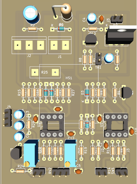
PCB Layout Strategies to Mitigate Noise Issues
Introduction
Printed Circuit Board (PCB) design plays a crucial role in ensuring the performance and reliability of electronic systems. One of the most significant challenges in PCB design is managing noise, which can degrade signal integrity, introduce electromagnetic interference (EMI), and lead to system malfunctions. Noise in PCBs can originate from various sources, including power supply fluctuations, high-speed signal switching, crosstalk, and ground loops.
This article explores key PCB layout techniques to minimize noise and enhance signal integrity. By implementing proper grounding, power distribution, signal routing, and shielding strategies, designers can significantly reduce noise-related issues in their circuits.
1. Understanding Noise Sources in PCBs
Before addressing noise mitigation techniques, it is essential to identify common noise sources in PCB designs:
1.1 Power Supply Noise
- Switching regulators and DC-DC converters introduce ripple and transient noise.
- Poor decoupling capacitor placement can lead to voltage fluctuations.
1.2 Signal Integrity Issues
- High-speed digital signals (e.g., clock lines, data buses) generate electromagnetic interference (EMI).
- Impedance mismatches cause signal reflections and ringing.
1.3 Crosstalk
- Adjacent traces carrying high-frequency signals induce unwanted coupling.
- Poor spacing and parallel routing increase crosstalk.
1.4 Ground Loops and Ground Noise
- Inconsistent ground return paths create voltage differences.
- High-current return paths interfere with sensitive analog circuits.
1.5 Radiated and Conducted EMI
- High-frequency signals radiate electromagnetic waves.
- Poor filtering allows noise to propagate through power and signal lines.

2. PCB Layout Techniques to Reduce Noise
2.1 Proper Grounding Strategies
2.1.1 Use a Solid Ground Plane
- A continuous ground plane provides a low-impedance return path for signals.
- Avoid splitting ground planes unless necessary (e.g., separating analog and digital grounds).
2.1.2 Star Grounding for Mixed-Signal Designs
- Connect analog and digital grounds at a single point to prevent ground loops.
- Use ferrite beads or 0Ω resistors for isolation if needed.
2.1.3 Minimize Ground Loops
- Ensure high-current return paths do not interfere with sensitive circuits.
- Keep ground traces short and wide to reduce inductance.
2.2 Power Distribution Network (PDN) Optimization
2.2.1 Decoupling Capacitors Placement
- Place decoupling capacitors as close as possible to IC power pins.
- Use multiple capacitors (e.g., 0.1µF, 1µF, 10µF) to filter different noise frequencies.
2.2.2 Power Plane Segmentation
- Separate noisy power domains (e.g., digital, analog, RF) using split power planes.
- Use ferrite beads or inductors for isolation between power sections.
2.2.3 Low-Inductance Power Traces
- Use wide traces or power planes to minimize parasitic inductance.
- Avoid long, thin power traces that increase impedance.
2.3 Signal Routing Best Practices
2.3.1 Controlled Impedance Routing
- Match trace impedance to the source and load (e.g., 50Ω for RF, 90Ω for differential pairs).
- Use microstrip or stripline configurations for high-speed signals.
2.3.2 Minimize Crosstalk
- Increase spacing between parallel traces (3x trace width is a good rule).
- Route high-speed signals orthogonally to reduce coupling.
- Use guard traces or ground shielding between sensitive signals.
2.3.3 Avoid Sharp Bends in High-Speed Traces
- Use 45° or curved traces instead of 90° turns to reduce reflections.
2.4 Shielding and EMI Reduction
2.4.1 Use Grounded Copper Pours
- Fill unused PCB areas with grounded copper to reduce EMI radiation.
- Connect copper pours to the ground plane with multiple vias.
2.4.2 Enclosure Shielding
- Use metal shielding cans for sensitive RF or analog circuits.
- Ensure proper grounding of shielding materials.
2.4.3 Filtering Noise at Connectors
- Add ferrite beads or common-mode chokes near I/O connectors.
- Use EMI filters on power and signal lines entering/leaving the PCB.
2.5 Component Placement for Noise Reduction
2.5.1 Separate Analog and Digital Components
- Keep analog circuits (e.g., sensors, ADCs) away from digital noise sources (e.g., microcontrollers, switching regulators).
2.5.2 Orient High-Speed Components Carefully
- Place clock generators and high-speed transceivers away from sensitive analog sections.
- Use shielding if necessary.
2.5.3 Thermal Management
- Heat from power components can affect noise performance.
- Ensure proper heat sinking and airflow to maintain stable operation.

3. Advanced Noise Reduction Techniques
3.1 Differential Signaling
- Use differential pairs (e.g., USB, Ethernet) for noise immunity.
- Maintain consistent trace length and spacing to prevent skew.
3.2 Spread Spectrum Clocking (SSC)
- Reduces peak EMI by modulating the clock frequency.
- Useful for high-speed digital systems.
3.3 Via Optimization
- Use multiple vias for ground connections to reduce inductance.
- Avoid via stubs in high-frequency signal paths.
3.4 Simulation and Testing
- Perform signal integrity (SI) and power integrity (PI) simulations before fabrication.
- Use spectrum analyzers and oscilloscopes to measure noise in prototypes.
4. Conclusion
Noise in PCB designs can significantly impact system performance, but with careful layout techniques, most noise-related issues can be mitigated. Key strategies include:
- Implementing proper grounding and power distribution.
- Optimizing signal routing to minimize crosstalk and reflections.
- Using shielding and filtering to reduce EMI.
- Separating noisy and sensitive circuit sections.
By following these best practices, PCB designers can achieve robust, low-noise designs suitable for high-performance applications. Continuous testing and simulation further ensure that noise is minimized before mass production.
