PCB Multilayer Boards: Flux Cancellation Method for Effective EMC Control
Abstract
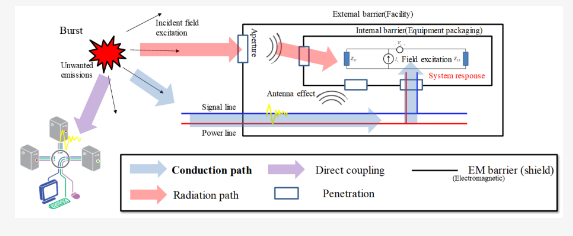
Electromagnetic compatibility (EMC) is a critical concern in the design of modern printed circuit boards (PCBs), especially in high-speed and high-frequency applications. Multilayer PCBs are widely used to enhance signal integrity and reduce electromagnetic interference (EMI). One effective technique for controlling EMC in multilayer PCBs is the flux cancellation method, which minimizes radiated emissions by exploiting opposing current flows in adjacent layers. This paper explores the principles of flux cancellation, its implementation in multilayer PCBs, and its effectiveness in EMC control. Key design considerations, including layer stack-up, return path management, and differential signaling, are discussed to optimize EMC performance.
1. Introduction
With the increasing complexity and speed of electronic circuits, managing electromagnetic interference (EMI) has become a significant challenge in PCB design. Multilayer PCBs offer improved signal integrity and reduced EMI compared to single or double-layer boards. However, improper layer arrangement and current return paths can lead to increased radiated emissions, degrading EMC performance.
The flux cancellation method leverages the natural behavior of current flow in adjacent PCB layers to minimize electromagnetic emissions. By ensuring that forward and return currents are closely coupled, the magnetic fields generated by these currents cancel each other out, reducing overall EMI. This paper examines the theoretical basis of flux cancellation, practical implementation techniques, and design guidelines to maximize its effectiveness.
2. Principles of Flux Cancellation
2.1 Magnetic Field Generation in PCBs
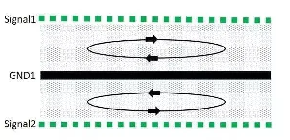
When current flows through a PCB trace, it generates a magnetic field around the conductor. In a multilayer PCB, if the return current follows a different path than the forward current, the resulting loop area between the two currents can act as an antenna, radiating EMI.
2.2 Flux Cancellation Mechanism
Flux cancellation occurs when two parallel conductors carry equal and opposite currents. The magnetic fields generated by these currents oppose each other, leading to partial or complete cancellation. In a multilayer PCB, this can be achieved by:
- Placing signal and return paths on adjacent layers.
- Using tightly coupled differential pairs.
- Ensuring a low-impedance return path for high-frequency signals.
2.3 Current Return Path Considerations
For flux cancellation to be effective, the return current must follow the path of least impedance, which, at high frequencies, is directly beneath the signal trace. Proper ground plane placement is crucial to minimize loop area and maximize field cancellation.
3. Implementation in Multilayer PCBs
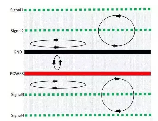
3.1 Layer Stack-up Design
An optimized layer stack-up is essential for effective flux cancellation. Common configurations include:
- 4-Layer PCB: Signal – Ground – Power – Signal
- 6-Layer PCB: Signal – Ground – Signal – Power – Ground – Signal
- 8-Layer PCB: Signal – Ground – Signal – Power – Ground – Signal – Power – Signal
Key guidelines:
- Place high-speed signal layers adjacent to solid ground planes.
- Avoid splitting ground planes, as this disrupts return paths.
- Use power planes as return paths for AC signals.
3.2 Differential Signaling
Differential pairs inherently utilize flux cancellation because the currents in the two traces are equal and opposite. Proper routing techniques include:
- Maintaining consistent trace spacing and length.
- Routing differential pairs over an unbroken reference plane.
- Avoiding sharp bends and vias that introduce impedance mismatches.
3.3 Decoupling and Grounding Strategies
- Use decoupling capacitors near IC power pins to minimize high-frequency noise.
- Implement a low-inductance grounding scheme to ensure effective return current paths.
- Avoid ground loops by using a single-point or multi-point grounding strategy, depending on frequency.
4. Effectiveness in EMC Control
4.1 Reduction in Radiated Emissions
By minimizing loop area and ensuring opposing currents, flux cancellation significantly reduces radiated emissions. Measurements show that proper implementation can achieve 10-20 dB reduction in EMI levels.
4.2 Improved Signal Integrity
Flux cancellation also enhances signal integrity by reducing crosstalk and reflections. Controlled impedance routing further ensures minimal signal distortion.
4.3 Compliance with EMC Standards
Properly designed multilayer PCBs using flux cancellation techniques can meet stringent EMC standards such as:
- FCC Part 15 (for unintentional radiators).
- CISPR 22/32 (for IT equipment).
- IEC 61000-4 (for immunity and emissions).
5. Practical Design Considerations
5.1 Trace Routing Best Practices
- Route high-speed signals over continuous reference planes.
- Minimize layer transitions to reduce discontinuities in return paths.
- Use microstrip or stripline configurations for controlled impedance.
5.2 Via Optimization
- Use ground vias near signal vias to provide a low-impedance return path.
- Avoid excessive via stubs, which can cause signal reflections.
5.3 Simulation and Testing
- Perform EMC simulations (e.g., using Ansys HFSS or CST Studio) to predict radiated emissions.
- Conduct near-field and far-field EMI testing to validate design performance.
6. Case Study: Flux Cancellation in a High-Speed PCB
A case study involving a 6-layer high-speed digital PCB demonstrated that implementing flux cancellation reduced radiated emissions by 15 dB at 1 GHz. Key improvements included:
- Adjacent signal and ground layers for tight coupling.
- Differential pair routing with minimized spacing.
- Optimized decoupling capacitor placement.
7. Conclusion
The flux cancellation method is a highly effective technique for controlling EMC in multilayer PCBs. By carefully designing layer stack-ups, ensuring proper return paths, and utilizing differential signaling, designers can significantly reduce EMI and improve signal integrity. Future advancements in PCB materials and simulation tools will further enhance the effectiveness of flux cancellation in high-frequency applications.