Common PCB Design Process Vulnerabilities and How to Mitigate Them
Introduction
Printed Circuit Board (PCB) design is a complex process involving multiple stages, from schematic capture to layout, manufacturing, and testing. Despite advancements in design tools and fabrication techniques, various process vulnerabilities can lead to defects, reliability issues, or even complete PCB failures. These vulnerabilities may arise from design errors, material selection, manufacturing limitations, or testing oversights.
This article explores the most common PCB design process vulnerabilities, their root causes, and best practices to mitigate them.
1. Poor Schematic Design and Component Selection
Vulnerabilities:
- Incorrect component footprints: Using wrong footprints (e.g., mismatched pad sizes) leads to assembly issues.
- Inadequate power supply design: Insufficient decoupling capacitors or improper voltage regulation causes noise and instability.
- Unoptimized signal integrity: Poorly designed high-speed traces result in signal reflections, crosstalk, and EMI.
Mitigation Strategies:
- Verify component footprints against datasheets before finalizing the design.
- Perform power integrity simulations to ensure stable voltage distribution.
- Follow high-speed design rules (impedance matching, proper termination).
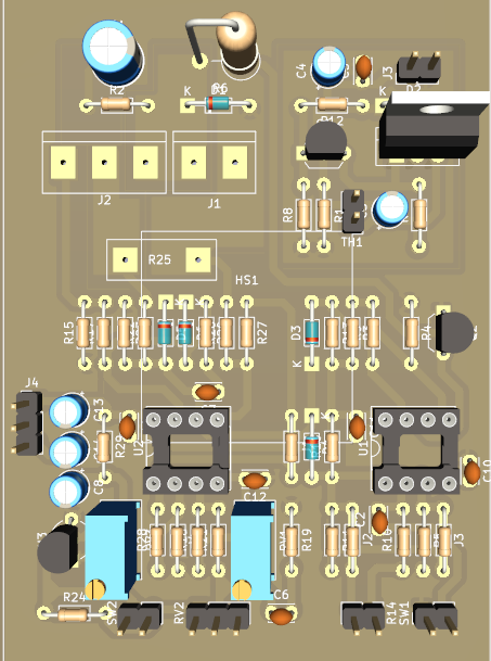
2. Layout-Related Vulnerabilities
Vulnerabilities:
- Improper trace routing:
- Insufficient clearance between high-voltage traces.
- Long parallel traces causing crosstalk.
- Sharp 90° angles leading to impedance discontinuities.
- Thermal management issues:
- Inadequate copper pours or thermal vias for heat dissipation.
- Poor placement of heat-generating components.
- Grounding problems:
- Split ground planes causing ground loops.
- Insufficient return paths for high-frequency signals.
Mitigation Strategies:
- Use 45° or curved traces instead of sharp 90° bends.
- Implement proper spacing rules for high-voltage and high-frequency signals.
- Use solid ground planes and avoid splits in critical return paths.
- Add thermal vias and heatsinks for power components.
3. Manufacturing Process Vulnerabilities
Vulnerabilities:
- Insufficient Design for Manufacturability (DFM):
- Too-small drill holes or annular rings causing fabrication failures.
- Inadequate solder mask clearance leading to solder bridges.
- Copper imbalance: Uneven copper distribution causes warping during reflow.
- Poor via design:
- Micro-vias without proper plating leading to cracks.
- Insufficient via tenting causing solder wicking.
Mitigation Strategies:
- Follow PCB manufacturer’s DFM guidelines for minimum trace width, spacing, and hole sizes.
- Balance copper distribution across layers to prevent warping.
- Use tented vias to prevent solder migration.
4. Assembly and Soldering Defects
Vulnerabilities:
- Solder joint failures:
- Cold solder joints due to improper reflow profiles.
- Tombstoning of small components (e.g., resistors, capacitors).
- Component misalignment:
- Incorrect pick-and-place machine calibration.
- Poorly designed pad geometries.
- Moisture sensitivity:
- Delamination or “popcorning” in ICs due to absorbed moisture.
Mitigation Strategies:
- Optimize reflow soldering profiles based on component requirements.
- Use proper pad geometries (e.g., thermal relief pads for large components).
- Store moisture-sensitive components in dry environments and pre-bake if necessary.

5. Signal Integrity and EMI Issues
Vulnerabilities:
- Inadequate EMI shielding:
- Poor grounding of shielding cans.
- High-frequency noise coupling into sensitive circuits.
- Impedance mismatches:
- Uncontrolled impedance traces in high-speed designs.
- Mismatched differential pairs causing signal degradation.
Mitigation Strategies:
- Use ground planes and shielding techniques (e.g., Faraday cages).
- Simulate signal integrity before fabrication (e.g., using HyperLynx or SIwave).
- Maintain consistent impedance in high-speed traces (e.g., USB, PCIe).
6. Testing and Quality Control Gaps
Vulnerabilities:
- Insufficient test coverage:
- Missing test points for critical signals.
- Lack of automated optical inspection (AOI) in production.
- Environmental stress failures:
- Undetected thermal cycling or vibration weaknesses.
Mitigation Strategies:
- Include test points for key signals (power, ground, high-speed lines).
- Implement Design for Testability (DFT) principles.
- Conduct environmental stress testing (HALT/HASS) for reliability validation.
Conclusion
PCB design vulnerabilities can arise at any stage—schematic design, layout, manufacturing, assembly, or testing. By understanding these common pitfalls and implementing best practices such as DFM checks, signal integrity simulations, and rigorous testing, designers can significantly reduce the risk of failures.
Adopting a proactive approach—leveraging simulation tools, collaborating with manufacturers, and adhering to industry standards—ensures robust and reliable PCB designs. Continuous improvement in design processes will further minimize vulnerabilities, leading to higher-quality electronic products.