The Significance of Copper Pour in PCB Design
Abstract
Printed Circuit Board (PCB) design is a critical aspect of modern electronics, influencing performance, reliability, and manufacturability. One of the essential techniques in PCB layout is copper pour (also known as copper flooding or ground plane). This paper explores the significance of copper pour in PCB design, discussing its benefits in terms of signal integrity, thermal management, electromagnetic interference (EMI) reduction, and manufacturability. Additionally, potential challenges and best practices for implementing copper pour are examined.
1. Introduction
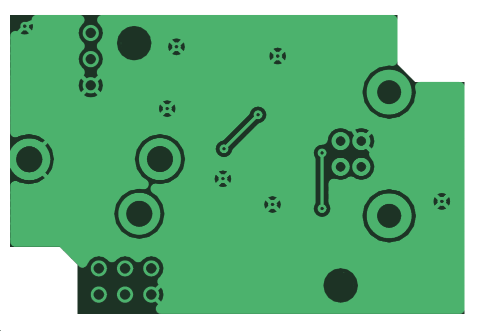
Copper pour refers to the process of filling unused areas of a PCB with solid or hatched copper, typically connected to a ground or power net. This technique is widely used in both single-layer and multi-layer PCBs to enhance electrical performance and structural stability. The strategic application of copper pour can significantly impact a PCB’s functionality, making it a crucial consideration in high-speed, high-frequency, and high-power designs.
2. Key Benefits of Copper Pour
2.1 Improved Signal Integrity
Signal integrity (SI) is vital in high-speed digital and RF circuits. Copper pour helps in several ways:
- Reduces Ground Noise: A continuous ground plane minimizes ground loops and provides a low-impedance return path for signals.
- Controls Impedance: In high-frequency designs, controlled impedance traces require a consistent reference plane. Copper pour ensures uniform impedance, reducing signal reflections and crosstalk.
- Minimizes Electromagnetic Interference (EMI): By acting as a shield, copper pour reduces radiated emissions and susceptibility to external noise.
2.2 Enhanced Thermal Management
Heat dissipation is a critical concern in PCBs, especially in power electronics and high-current applications. Copper pour aids thermal management by:
- Distributing Heat Evenly: Copper has high thermal conductivity, helping spread heat away from hot components.
- Improving Heat Sinking: Large copper areas connected to power components (e.g., MOSFETs, regulators) act as heat spreaders, reducing thermal resistance.
- Supporting Thermal Vias: Copper pour works with thermal vias to transfer heat to inner layers or the opposite side of the PCB.
2.3 EMI and Noise Reduction
Electromagnetic interference (EMI) can degrade performance and cause compliance issues. Copper pour mitigates EMI by:
- Shielding Sensitive Traces: Surrounding high-speed or analog signals with grounded copper reduces capacitive and inductive coupling.
- Reducing Loop Area: A solid ground plane minimizes current loop areas, lowering radiated emissions.
- Preventing Antenna Effects: Unconnected copper islands can act as antennas; proper grounding avoids this issue.
2.4 Manufacturing and Mechanical Benefits
Copper pour also improves PCB manufacturability and structural integrity:
- Balances Copper Distribution: Prevents warping during fabrication by ensuring even copper distribution across layers.
- Reduces Etching Time: Less copper to etch means faster production and lower costs.
- Strengthens the Board: Additional copper increases mechanical rigidity, reducing the risk of flexing or cracking.
3. Challenges and Considerations
While copper pour offers numerous advantages, improper implementation can lead to issues:
3.1 Ground Loops and Stubs
- If copper pour is not properly connected, it can create unintended ground loops or floating copper stubs, leading to noise and signal integrity problems.
3.2 Increased Parasitic Capacitance
- Excessive copper near high-frequency signals may introduce parasitic capacitance, affecting signal rise times and impedance matching.
3.3 Thermal Expansion Mismatch
- Large copper areas can cause uneven thermal expansion, leading to mechanical stress on components.
3.4 Acid Traps in Manufacturing
- Narrow gaps in copper pour can trap etching chemicals, leading to manufacturing defects.
4. Best Practices for Copper Pour Implementation
To maximize benefits while minimizing drawbacks, designers should follow these guidelines:
4.1 Proper Grounding Strategy
- Ensure copper pour is well-connected to the ground net with multiple vias to avoid floating copper.
- Use a solid ground plane in multi-layer PCBs for optimal return paths.
4.2 Thermal Relief Connections
- For component pads connected to copper pour, use thermal relief spokes to prevent heat dissipation issues during soldering.
4.3 Avoiding Antenna Effects
- Eliminate isolated copper islands by connecting them to a net or removing them entirely.
4.4 Controlled Copper Spacing
- Maintain adequate clearance between copper pour and high-voltage traces to prevent arcing.
4.5 Use of Hatched Copper
- In some cases, hatched (gridded) copper can reduce weight and improve flexibility while still providing EMI benefits.
5. Conclusion
Copper pour is a fundamental technique in PCB design, offering significant advantages in signal integrity, thermal management, EMI reduction, and manufacturability. However, improper application can introduce challenges such as parasitic capacitance, ground loops, and manufacturing defects. By adhering to best practices—such as proper grounding, thermal relief, and controlled spacing—designers can optimize copper pour for enhanced PCB performance and reliability.
As electronics continue to evolve with higher speeds and greater power demands, the strategic use of copper pour will remain a critical factor in successful PCB design.